
Quick Answer: Tachyon 100G is an ultra-low loss hydrocarbon-thermoset laminate designed for 100+ Gbps digital routing, featuring a stable Dk of 3.02 and a Df of 0.0021 at 10 GHz. It processes similarly to standard FR-4 without requiring plasma desmear, cutting insertion loss by 35% compared to Megtron 6 at 16 GHz. Key takeaways:
- Dissipation factor remains extremely stable at 0.0021 up to 100 GHz.
- Lamination strictly requires prepreg moisture control under 40% RH.
- It operates flawlessly in hybrid stackups paired with Astra MT77.
- Material costs average 3 to 5 times higher than standard mid-Tg laminates.
Table of Contents
- #1 What Makes Tachyon 100G the Benchmark for 100Gbps PCB Designs?
- #2 What Electrical Properties Define Its High-Frequency Performance?
- #3 How Do Thermal and Mechanical Specs Affect Board Reliability?
- #4 Why Do HVLP Copper and Spread Glass Matter for This Laminate?
- #5 How Does Tachyon 100G Compare to Megtron 6 and TerraGreen?
- #6 When Should You Build a Tachyon 100G + Astra MT77 Hybrid Stackup?
- #7 What Stackup Design Rules Apply to Ultra-Low Loss Boards?
- #8 How Do Fabricators Process This Material in Production?
- #9 Which Applications Actually Justify the Cost of Tachyon 100G?
- #10 How Do You Qualify a PCB Manufacturer for High-Speed Builds?
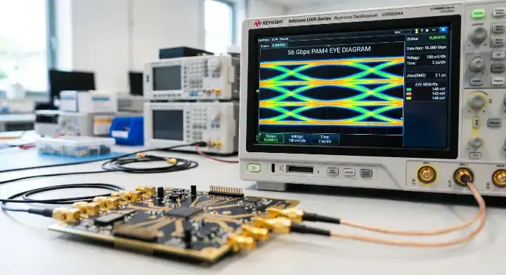
You are laying out a 56 Gbps PAM4 switch backplane, and signal integrity simulations show your channel budget collapsing before the signal even reaches the connector. Pushing signals past 25 Gbps on standard materials creates massive insertion loss and timing skew, forcing layout engineers to add expensive retimers just to keep the eye diagram open. The solution is moving to a true ultra-low loss laminate like Tachyon 100G. This specific substrate slashes signal attenuation without forcing your fabricator into exotic PTFE processing methods.
1. What Makes Tachyon 100G the Benchmark for 100Gbps PCB Designs?
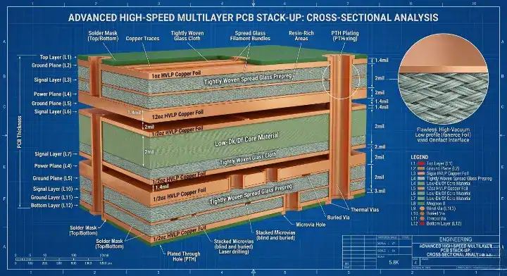
Tachyon 100G is a hydrocarbon-thermoset laminate designed specifically for high-speed digital applications above 10 GHz, supporting protocol speeds like 100G, 400G, and 800G Ethernet. Per IPC-4103 slash sheet /17, this material is classified as a low-loss dielectric that reliably survives up to 10 sequential lamination cycles.
Why Is the Updated Version Different?
Here is the technical breakdown:
- Z-Axis Expansion: The upgraded version improves Z-axis coefficient of thermal expansion by 30% over the original formulation.
- Pitch support: It comfortably supports BGA pitches of 0.8 mm or smaller without fracturing internal vias.
- Material baseline: By analyzing FR-4 material properties and Tg grades, you quickly see standard boards cannot match its 215°C Tg rating.
Bottom line: Select this specific laminate when your digital design crosses the 25 Gbps threshold and standard multilayer boards repeatedly fail your insertion loss limits.
2. What Electrical Properties Define Its High-Frequency Performance?
The electrical performance of this laminate revolves around its tight Dielectric Constant (Dk) of 3.02 and Dissipation Factor (Df) of 0.0021 at 10 GHz. Per the official Isola Group Datasheet, the dissipation factor remains incredibly stable at 0.0021 across a massive temperature range of -55°C to +125°C.
How Does Frequency Scaling Work?
Df (dissipation factor) is the ratio of energy dissipated to energy stored per cycle in a dielectric material. This substrate’s Df of 0.0021 stays flat all the way up to 100 GHz, preventing sudden high-frequency signal drop-offs.
Consider the physical reality:
- Signal stability: Flat Dk responses mean less phase noise on high-speed differential pairs running long physical distances.
- Broadband transmission: The engineered resin reduces signal dispersion at millimeter-wave frequencies.
Bottom line: Rely on this ultra-low loss dielectric for 56 Gbps PAM4 or 112G designs where physical trace length dictates your total channel attenuation budget.
3. How Do Thermal and Mechanical Specs Affect Board Reliability?
Thermal stability defines how a PCB survives assembly, and this material delivers a primary Tg (Glass Transition Temperature) of 215°C via DSC testing. The Z-axis Coefficient of Thermal Expansion (CTE) measures 45 ppm/°C pre-Tg and 250 ppm/°C post-Tg, resulting in a total expansion of just 2.5% from 50°C to 260°C.
What Limits Plated Through-Hole Reliability?
Time to Delamination (T288) is the precise time a laminate survives at 288°C before physical layer separation occurs. This substrate achieves a T288 greater than 60 minutes, giving your high-speed PCB fabrication capability an enormous safety margin.
Look at the thermal limits:
- T260 > 60 minutes to handle multiple thick-board reflow passes.
- T300 > 20 minutes for extreme assembly environments.
- Td (Decomposition Temperature): 360°C at 5% weight loss.
Bottom line: Specify this laminate for high-layer-count boards with multiple thermal excursions, as its 2.5% Z-axis expansion prevents microvia cracking during lead-free reflow.
4. Why Do HVLP Copper and Spread Glass Matter for This Laminate?
High-frequency signal transmission relies on perfectly smooth copper, so this material uses HVLP, HVLP3, or RTF copper foils with an Rz roughness of exactly 1.0 to 2.5 µm. It combines this with spread weave glass styles like 1035, 1067, 1078, 1086, and 3313 to entirely eliminate the destructive fiber weave effect.
How Does Copper Roughness Kill High-Speed Signals?
The skin effect is a phenomenon where high-frequency alternating current concentrates entirely near the outer surface of a conductor. When copper roughness (Rz) exceeds 2.5 µm, the signal travels along microscopic peaks and valleys, increasing attenuation by up to 15%.
Let’s look at the construction:
- Spread glass: Mechanically flattens glass bundles to prevent Dk variations over short physical distances on a trace.
- HVLP3 copper: Provides an ultra-flat surface profile near 1.0 µm for flawless 100+ Gbps lane performance.
Bottom line: Always explicitly specify HVLP copper and spread glass weaves on your fabrication notes; standard ED copper will completely negate the electrical benefits of the low-loss resin.
5. How Does Tachyon 100G Compare to Megtron 6 and TerraGreen?
In a 56 Gbps PAM4 channel across 15 inches of trace, swapping from Megtron 6 to Tachyon 100G mathematically reduces your insertion loss by 26% to 43% depending on the exact frequency. At 16 GHz, physical test vehicles demonstrate that this material provides a 35% better insertion loss profile than Panasonic’s Megtron 6.
Does the 0.5 dB Difference Actually Matter?
A severe DFM review often reveals that designers misunderstand channel loss accumulation over long backplane routes.
Here is the truth about channel budgets:
- Megtron 6 comparison: Per IEEE 802.3 100GEL Task Force data, a 9-inch host trace on Megtron 6 consumes 14 dB at 28 GHz; the newer Isola material cuts this significantly.
- Megtron 7: Panasonic’s direct competitor matches the 0.0021 Df but features a lower Tg rating.
- TerraGreen 400G: A halogen-free alternative with slightly lower Df values for environmentally restricted designs.
Bottom line: Upgrade to the Isola material when your simulated 56 Gbps channel loss exceeds your budget by 1 to 2 dB and you cannot physically shorten the trace length.
6. When Should You Build a Tachyon 100G + Astra MT77 Hybrid Stackup?
Building a hybrid stackup with Tachyon 100G and Astra MT77 is highly viable because both materials share perfectly matched CTE profiles from -55°C to +125°C. You process this combination in a single lamination cycle, using the high-speed material for digital routing and Astra for the RF/microwave layers.
Is Hybrid Lamination a Major Factory Risk?
A hybrid stackup is a multilayer board built using two distinct resin systems to isolate functional performance at a lower total cost. Mismatched CTEs normally warp boards during cooling, but these two materials match within 5% post-Tg expansion.
Watch out for these production hurdles:
- Layer transitions: Signal transitions between cores must mathematically account for the Dk mismatch (3.02 vs 3.0).
- Prepreg selection: Factories must use the correct binding prepreg to bond the discrete cores without delamination.
- Capability constraint: Fewer than 5% of global PCB shops possess the qualification to run this specific hybrid successfully.
Bottom line: Deploy this exact hybrid configuration for phased array radars or 5G mmWave modules where heavy digital processing sits directly beneath an RF antenna array.
7. What Stackup Design Rules Apply to Ultra-Low Loss Boards?
Designing a stackup with this ultra-low loss laminate requires keeping high-speed via stubs strictly under 8 mils and enforcing aggressive trace separation rules. Differential pair routing requires precision geometry across spread glass to maintain an 85-ohm or 100-ohm impedance profile within ±5%.
What Are the Key Layout Traps?
A via stub is the unused metallic portion of a plated through-hole that reflects high-frequency energy back toward the source. At 25+ Gbps, a stub longer than 8 mils creates a resonant frequency null that completely collapses the signal eye.
Protect your design using these methods:
- Backdrilling: Mandate precision backdrilling for all through-hole transitions to physically eliminate stubs.
- HDI PCB manufacturing: Utilize stacked microvias instead of through-holes to avoid creating stubs entirely.
Bottom line: Never release a 100Gbps layout without running full 3D electromagnetic simulations on every single via transition and connector launch geometry.
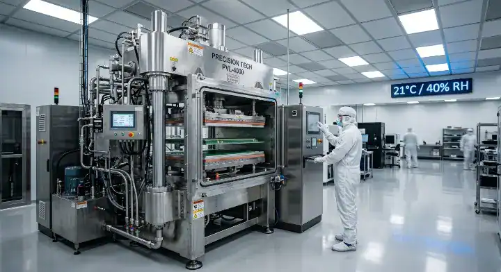
8. How Do Fabricators Process This Material in Production?
Processing this laminate is highly efficient because it requires absolutely no plasma desmear, relying entirely on standard FR-4 chemical permanganate desmear lines. The mechanical drilling parameters require lower chiploads and cutting speeds compared to standard FR-4, while the lamination cycle demands 60 minutes at 200°C.
What Happens When Prepreg Moisture Is Ignored?
Let me share a factory floor reality:
The first time our team processed a high-layer-count board for a 400G switch line card using this material, we lost two panels in lamination to delamination at the inner-layer cores. The root cause was prepreg moisture, as the lower resin flow leaves less margin for trapped moisture to escape during cure. We immediately restricted prepreg storage to a dedicated room held at 21°C and 40% RH, set a strict 168-hour shelf-life cap after opening the moisture barrier bag, and added a mandatory 30-minute, 100°C pre-bake on all layer pairs. Since tightening these controls, our first-pass yield on these panels consistently runs at 96%.
Bottom line: If a fabricator quotes this laminate using expensive PTFE processing fees or requires plasma desmear, they lack experience with the material system; find a new partner immediately.
9. Which Applications Actually Justify the Cost of Tachyon 100G?
The true cost of Tachyon 100G runs 3 to 5 times higher than standard mid-Tg FR-4 on a strictly layer-equivalent basis. You justify this extreme financial premium strictly for 100G/400G/800G switches, AI/HPC accelerators, router backplanes, PCIe 5.0/6.0 servers, and 5G AAU base stations.
These same 800G and 1.6T switch line cards are central to NVIDIA’s Blackwell platform—each NVL72 rack ships nine NVSwitch trays, each carrying two 28.8 Tb/s ASICs. For the full breakdown of how Tachyon 100G and M8-grade laminates coexist in a Blackwell-class BOM, see our NVIDIA Blackwell PCB material guide
Does the Bare Board Premium Save System Costs?
Consider this project outcome:
One of our recent builds was a 22-layer backplane for a customer designing a 400 Gb/s router line card. The board featured 4 oz internal power planes, 0.8 mm pitch BGAs, and 28 Gbps PAM4 SerDes routed via striplines. We applied HVLP3 copper on the SerDes layers and standard HVLP2 on lower-speed nets to optimize the budget. Insertion loss measured an incredibly low 0.61 dB/inch at 14 GHz on 4 mil traces. The final board price was 4.2x higher than FR-4, but the customer’s SI team confirmed the channel met the required budget without utilizing active retimers. That architectural simplification saved them roughly $80 per assembled system, making the bare board premium highly profitable.
Bottom line: Invest in this premium substrate only when removing expensive signal conditioning components offsets the bare board cost multiplier.
10. How Do You Qualify a PCB Manufacturer for High-Speed Builds?
To qualify a PCB manufacturer for ultra-low loss builds, you must verify they hold a qualified construction set and maintain active inventory of specific HVLP copper SKUs. Lead times for this raw material run 2 to 4 weeks from vendors, meaning shops without active stock will severely delay your prototype schedules.
What Checklist Should You Send Your Fab?
A Signal Integrity Test Vehicle (SI TV) is a standardized PCB layout used to extract bare-board insertion loss and impedance data directly from the factory floor before a production run. Asking a fab for their historical SI TV data proves their etching and pressing tolerances.
Here is the reality of vetting suppliers:
- Climate control verification: Ask for logs proving their prepreg storage maintains strictly <50% RH.
- Process capability: Request proof of sub-8 mil stub backdrilling and sequential lamination success rates.
- Material transparency: Confirm they understand when to down-spec to TerraGreen 400G for cost savings if halogen-free status is preferred.
Bottom line: Never trust a fabricator’s capability claim for 100Gbps materials unless they can provide physical measurement reports from previous signal integrity test vehicles.
The transition to 100Gbps and 400Gbps architectures unforgivingly exposes every flaw in your dielectric selection, copper roughness, and via stub management. By utilizing the ultra-low loss characteristics of this engineered substrate, you secure the insertion loss margins necessary to keep high-speed eyes wide open without resorting to costly PTFE processing. We solve complex signal integrity challenges by marrying aggressive DFM analysis with strictly controlled factory-floor execution. If you need to validate your next high-speed backplane or hybrid stackup, contact us today for a comprehensive engineering review. QueenEMS is committed to building the hardware infrastructure of tomorrow with precision you can measure.
Frequently Asked Questions
Can I use Tachyon 100G with standard FR-4 fabrication processes?
Yes. It is engineered to be processable on standard FR-4 equipment and strictly does not require plasma desmear. Drilling parameters use lower chiploads than standard FR-4, and lamination runs at 60 minutes at 200°C. If a fab quotes it like a PTFE material, they likely lack experience with the material.
What is the cost premium for this material versus standard FR-4?
On a layer-equivalent basis, expect 3 to 5 times the cost of standard mid-Tg FR-4. This is driven by raw material price, lower factory throughput, and tighter handling discipline. The premium narrows on high-layer-count boards where material becomes a smaller fraction of the total cost.
How do I know if my design actually needs this specific material?
If your channel runs at 25 Gbps NRZ or 56 Gbps PAM4 or above over traces longer than 8 inches, and your SI budget cannot accommodate a 14+ dB loss at the highest signal frequency, it is absolutely justified. Below 10 Gbps or under 6 inches of trace, lower-cost materials like I-Tera MT40 are typically sufficient.
What is the best material to pair with it in a hybrid stackup?
Astra MT77. Both materials share matched CTE behavior across -55°C to +125°C, validated at events like IMS2023. The high-speed digital layers utilize the 100G material, while Astra MT77 handles RF/microwave layers, making it highly useful in phased arrays and 5G mmWave designs.
How long does material lead time add to my PCB build schedule?
Expect 2 to 4 weeks of raw material lead time on top of standard fabrication time if your shop does not stock it. Pre-qualified fabs that hold material in stock can build in standard 3 to 4 week fab cycles. Confirm physical material availability before placing a time-critical build order.
Written by the QueenEMS Engineering Team
Upload your files today · Free DFM check before production · Ship worldwide
Get your PCB prototypes in as fast as 24 hours. We handle FR4, Rogers, and Flex up to 60 layers — free prototypes for 2–4 layer boards, no minimum order.
Just upload your Gerber + BOM — we source every part, assemble, and inspect (AOI + X‑Ray) so you don't have to chase suppliers. Boards ship in as fast as 24 hours.