
Routing 112 Gbps PAM4 signals across backplanes pushes standard FR-4 materials past their physical breaking point, resulting in massive signal distortion and thermal failure. Engineering teams face constant redesigns when trying to force legacy laminates into modern 800G environments. Shifting to an M8-grade architecture solves this physics constraint, and understanding the M9 CCL specification explained helps clarify why this tier remains the current volume standard. This guide details exactly how to utilize the industry’s leading ultra-low-loss laminate to stabilize your high-speed layouts.
Table of Contents
- What Makes R-5795 the M8-Grade Benchmark for AI Boards?
- What Electrical Properties Define Megtron 8 Laminates?
- How Do Thermal and Mechanical Specs Drive Board Reliability?
- Why Does This Material Pair Best with HVLP3 Copper?
- How Does Megtron 8 Compare to Legacy and M9 Generations?
- How Does R-5795 Stack Up Against EM-892K2 and SH G7?
- What Stackup Design Rules Apply to M8-Grade Boards?
- How Do Fabricators Process Megtron 8 in Production?
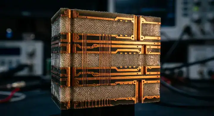
- Where Do These Laminates Show Up in GB200 and Switches?
- How Do You Qualify a Fab to Build Megtron 8 Volume?
What Makes R-5795 the M8-Grade Benchmark for AI Boards?
Why do procurement managers mistakenly use a specific product name to describe an entire material tier? The M8 standard represents NVIDIA’s internal classification for printed circuit boards requiring a dissipation factor of $\le 0.0015$ at $10\text{ GHz}$. Panasonic R-5795 hits $0.0010$, making it the de facto benchmark product that entirely defines the capabilities of this category.
Defining the M8 Standard
Hardware developers frequently confuse the private specification with the physical product itself. Here is the distinction:
- The grade is a performance requirement dictating maximum signal loss limits.
- R-5795 is a specific chemical formulation manufactured by Panasonic.
- Multiple vendors produce laminates capable of passing the M8 qualification. Key Takeaway: Separating the specification from the brand name gives your supply chain the flexibility to qualify alternative materials when allocations tighten.
Product Family Variations
The product line divides into specific part numbers depending on your exact routing needs. You will specify the standard laminate, a Low-Dk glass variant, or halogen-free options based on environmental compliance requirements. Key Takeaway: Check your bill of materials to confirm you are calling out the correct prepreg pairing for your selected core layers.
| Grade Level | Representative Product | Target Df | Market Status |
|---|---|---|---|
| M6 | Megtron 6 (R-5775) | $0.0020$ | H100 generation |
| M8 | R-5795 / EM-892K2 | $0.0010\text{-}0.0012$ | GB200 mainstream |
| M9 | DS-7409DYQ | $\le 0.0007$ | Rubin Ultra transition |
| Analysis: The progressive tightening of the dissipation factor defines the generational shift in high-speed hardware architecture. |
Bottom line: R-5795 serves as the definitive reference point for M8-class routing, but it remains one product inside a broader performance specification.
What Electrical Properties Define Megtron 8 Laminates?
What exact numbers justify selecting this material over cheaper alternatives? Per Panasonic’s official MEGTRON 8 product documentation, the R-5795 series delivers a Df of $0.0010\text{-}0.0012$ at $12\text{ GHz}$ and a Dk of $3.0\text{-}3.1$. These metrics produce approximately $30\%$ lower transmission loss compared to legacy generations, safely supporting 800GbE high-speed networking.
Core Electrical Specs
This ultra-low-loss profile relies on a specialized modified polyphenylene oxide (PPO) resin rather than standard epoxy. This chemical foundation prevents extreme frequency signals from bleeding into the surrounding dielectric material. Consider these factors:
- Dielectric constant stays incredibly stable across broad frequency sweeps.
- Lower Df directly correlates to a wider open data eye diagram.
- The resin formulation resists electrical breakdown under continuous high voltage. Key Takeaway: Verifying these electrical targets in your simulation software prevents costly impedance mismatches before Gerber files ever reach the factory floor.
Signal Loss Improvements
Minimizing pure signal attenuation remains the primary goal when designing boards with transceivers spaced far apart. If your team lacks internal modeling tools, use a PCB material selector tool to verify how these parameters interact with your trace widths. Key Takeaway: The raw reduction in insertion loss allows layout engineers to drop expensive retimer chips from the assembly.
| Electrical Metric | Value Range | Test Condition |
|---|---|---|
| Dk | $3.0\text{-}3.1$ | $10\text{-}12\text{ GHz}$ |
| Df | $0.0010\text{-}0.0012$ | $10\text{-}12\text{ GHz}$ |
| Transmission Loss vs M7 | $\approx 30\%$ Better | Factory Data |
| Analysis: Holding the Dk under 3.1 is absolutely critical for managing phase skew on differential pairs. |
Bottom line: The extreme reduction in signal attenuation provided by these specific Dk and Df values makes 112 Gbps PAM4 communication physically possible.
How Do Thermal and Mechanical Specs Drive Board Reliability?
Can this low-loss resin survive the brutal thermal cycling of a 24-layer pressing process? Yes, because the material features a glass transition temperature (Tg) of $220^\circ\text{C}$ and a decomposition temperature (Td) of $370^\circ\text{C}$. MEGTRON 8 R-5795 conforms to IPC-4101E slash sheets /102 and /91, guaranteeing high structural integrity during multi-press fabrication.
Managing Heat Profiles
Massive server motherboards endure immense thermal stress during component reflow and continuous operational field use. The exceptionally high Tg prevents the resin from softening and shearing the internal copper via barrels. Review the mechanical data:
- Z-axis CTE measures a highly stable $38\text{ ppm/}^\circ\text{C}$ below Tg.
- Total Z-axis expansion restricts to $1.5\%$ between $50^\circ\text{C}$ and $260^\circ\text{C}$.
- UL 94 V-0 ratings certify strict flammability compliance. Key Takeaway: Specifying materials with tight Z-axis expansion directly prevents catastrophic microvia cracking during the assembly phase.
Structural Integrity
The modified PPO resin provides a far more rigid mechanical structure than soft PTFE-based microwave boards. This rigidity supports heavy BGA components and dense heatsink mounting without dangerous substrate warping. Key Takeaway: Your mechanical engineering team must account for the specific CTE values of this material when designing the server chassis mounting points.
| Thermal Parameter | Metric | Test Method |
|---|---|---|
| Tg | $220^\circ\text{C}$ | DSC |
| Td | $370^\circ\text{C}$ | $5\%$ wt loss |
| Z-axis CTE | $38\text{ ppm/}^\circ\text{C}$ | $<\text{Tg}$ |
| Analysis: Keeping Z-axis expansion tightly controlled is the only way to yield reliable 20-layer boards with stacked microvias. |
Bottom line: The thermal stability of this laminate guarantees that the board maintains its electrical performance even when operating near maximum GPU heat limits.
Why Does This Material Pair Best with HVLP3 Copper?
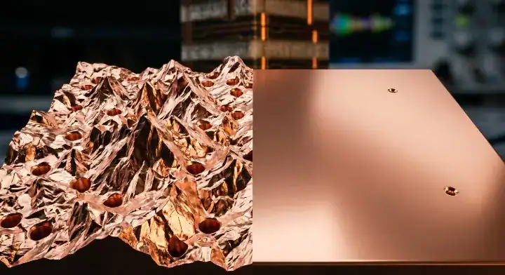
Why do fabricators reject standard copper foil on these high-end server backplanes? To harness the low Df of the resin, you must pair it with HVLP3 copper foil featuring a roughness (Rz) of $\le 1.0\ \mu\text{m}$. Standard rough copper forces the high-frequency signal to travel a longer physical path along the metal surface, completely ruining your insertion loss gains.
Mitigating the Skin Effect
As data rates climb, the signal energy concentrates intensely along the extreme outer boundary of the copper trace. If that boundary looks like a microscopic mountain range, the signal experiences massive resistive loss and phase delay. Look at the copper mechanics:
- Standard RTF copper creates severe attenuation above $10\text{ GHz}$.
- HVLP3 limits peak-to-valley roughness strictly under $1.0\ \mu\text{m}$.
- This ultra-smooth profile keeps 28 GHz insertion loss below $0.3\text{ dB/inch}$. Key Takeaway: Upgrading your resin chemistry provides zero benefit if you allow the factory to laminate the board with highly textured foil.
Glass Weave Selection
Beyond the copper, you must select NER-glass or Low-Dk spread glass to prevent the glass-weave skew effect. Traditional bundled glass fibers create periodic dielectric variations that cause timing mismatches across parallel data lanes. Key Takeaway: Specifying spread glass forces the manufacturer to use a flattened weave that creates a highly uniform dielectric baseline for precise differential routing.
| Copper Type | Max Rz Profile | Frequency Match |
|---|---|---|
| RTF | $\le 3.0\ \mu\text{m}$ | $< 10\text{ GHz}$ |
| HVLP2 | $\le 1.5\ \mu\text{m}$ | $\approx 14\text{ GHz}$ |
| HVLP3 | $\le 1.0\ \mu\text{m}$ | $28\text{ GHz}+$ |
| Analysis: Driving copper roughness toward an absolute flat mirror finish reclaims the final percentage points of your signal margin. |
Bottom line: Extracting the true value of M8-class laminates absolutely requires mandating ultra-smooth HVLP3 copper and uniform spread-glass reinforcements.
How Does Megtron 8 Compare to Legacy and M9 Generations?
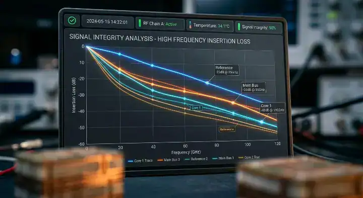
Is the $30\%$ transmission loss improvement over legacy materials worth the massive cost premium for your project? The answer depends on your trace length: M8-grade runs roughly $0.50\text{-}0.55\text{ dB/inch}$ at $28\text{ GHz}$, whereas the older generation sits near $0.72\text{ dB/inch}$. Per IEEE 802.3 800GBASE specifications, this exact delta dictates whether an 800G channel closes successfully without active amplification.
Is the Loss Improvement Worth It?
If your design runs 56 Gbps PAM4 over traces shorter than 12 inches, older M7 materials are entirely sufficient. When trace lengths push past 15 inches, or rates hit 112 Gbps PAM4, the legacy materials consume your entire 14 dB loss budget instantly. Evaluate your budget:
- The material carries a $30\text{-}50\%$ premium over previous generations.
- It saves roughly 2 to 4 dB of margin over a 20-inch trace.
- Upgrading to low-loss laminate manufacturing removes the need for costly retimers. Key Takeaway: Run your channel simulations strictly against trace length; short layouts do not economically justify the M8 material upgrade.
Cost Versus Performance Scaling
Looking ahead, the M9 generation drops loss further but introduces extreme processing challenges by utilizing quartz fiber. The current M8 baseline represents the absolute sweet spot for mass-producible AI hardware without triggering specialized cleanroom allocation fees. Key Takeaway: Stick to this generation for high-volume 800G builds, reserving M9 purely for experimental sub-systems or extreme backplanes.
| Laminate Grade | Attenuation @ 28 GHz | Cost Multiplier | Best Application |
|---|---|---|---|
| M6 Grade | $\approx 0.90\text{ dB/inch}$ | 1.0x | Prototype / Short run |
| M7 Grade | $\approx 0.72\text{ dB/inch}$ | 1.5x | Mid-tier server |
| M8 Grade | $\approx 0.52\text{ dB/inch}$ | 2.0x+ | 800G / AI server |
| Analysis: The cost multiplier strictly tracks the reduction in dB loss, proving that SI margin is the most expensive commodity in PCB design. |
Bottom line: The 30% loss improvement justifies the cost premium only when traversing long channels at 56 Gbps PAM4 or above; otherwise, legacy materials suffice.
How Does R-5795 Stack Up Against EM-892K2 and SH G7?
Can a procurement team substitute alternative M8-grade laminates to break free from aggressive supply chain allocations? EM-892K2, SH G7, and DS-7409DJN+ all classify as M8 alternatives, delivering Df values between $0.0013$ and $0.0015$. While Panasonic holds the benchmark, these competitors offer legitimate SI performance with drastically improved lead times for specific hyperscaler builds.
Can EM-892K2 or SH G7 Replace R-5795?
NVIDIA already qualifies EM-892K2 and DS-7409DJN+ for specific Blackwell platform layers to distribute supply chain risk. Shengyi’s SH G7 provides a massive price advantage—roughly $60\text{-}70\%$ of the benchmark cost—making it highly attractive for cost-sensitive domestic AI projects. Review the substitution rules:
- EM-892K2 matches performance closely and holds major AI qualifications.
- SH G7 reduces cost significantly but loses minor margin at 28 GHz.
- Substitutes must still hit Tg $\ge 200^\circ\text{C}$ and match Z-CTE limits. Key Takeaway: You can safely substitute these alternatives on non-critical routing layers, preserving the premium material purely for the longest SerDes channels.
Analyzing the Alternatives
Switching vendors requires a complete re-simulation of your stackup, as slight variations in Dk will alter your differential impedance targets. Working with a factory that actively stocks these alternatives protects your prototype schedule from unexpected OEM allocation lockouts. Key Takeaway: Demand coupon-level S-parameter data from your fabricator to prove the substitute material mathematically closes your channel budget.
| M8 Competitor | Dk @ 10 GHz | Df @ 10 GHz | Tg Value |
|---|---|---|---|
| Panasonic R-5795 | 3.0 | $0.0010\text{-}0.0012$ | $220^\circ\text{C}$ |
| EMC EM-892K2 | 3.0 | $0.0014$ | $210^\circ\text{C}$ |
| Shengyi SH G7 | 3.1 | $0.0014$ | $215^\circ\text{C}$ |
| Doosan DS-7409 | 3.0 | $0.0013$ | $220^\circ\text{C}$ |
| Analysis: The data shows that while competitors approach the benchmark Df, they generally sacrifice a few degrees of thermal rigidity to get there. |
Bottom line: In scenarios not completely starving for SI margin, EM-892K2 and DS-7409DJN+ serve as perfectly viable, production-ready substitutes for the benchmark laminate.
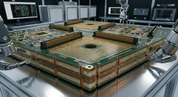
What Stackup Design Rules Apply to M8-Grade Boards?
How do engineering teams balance the extreme cost of these materials on massive 24-layer motherboards? They utilize hybrid stackup constructions, applying the premium M8 material exclusively to the outer signal layers while hiding cheaper M4 cores in the center. If your factory possesses true HDI PCB capability, they can seamlessly press these dissimilar resins together without delamination.
Routing for 112 Gbps
The premium laminate must surround the high-speed differential pairs on both the top and bottom to create a uniform dielectric field. Power delivery networks and low-speed digital control lines generate zero benefit from ultra-low Df materials. Follow these stackup principles:
- Route all 112 Gbps PAM4 signals exclusively on the premium layers.
- Assign power, ground, and I2C lines to M4-grade central cores.
- Balance the copper distribution perfectly to prevent asymmetric bowing. Key Takeaway: Isolating the expensive chemistry to the specific layers that require it can slash your total bare-board BOM cost by up to $40\%$.
Sequential Lamination Limits
Mixing materials requires matching the curing temperatures of both resin systems closely. Because M8-grade laminates mimic standard FR-4 pressing temperatures, fabricators execute multiple lamination cycles without thermally degrading the cheaper internal cores. Key Takeaway: Always request a verified pressing profile from your manufacturer to confirm the hybrid materials share compatible thermal expansion rates.
| Stackup Construction | High-Speed Layers | Power/GND Layers | Cost Impact |
|---|---|---|---|
| Full Premium Build | M8 Grade | M8 Grade | $100\%$ Baseline |
| Hybrid Build | M8 Grade | M4 Grade | $\approx 65\%$ Baseline |
| Analysis: The hybrid approach proves that intelligent mechanical design directly solves aggressive procurement budget constraints. |
Bottom line: Executing a hybrid stackup correctly maximizes signal integrity on the critical nets while aggressively managing the total manufacturing expenditure.
How Do Fabricators Process Megtron 8 in Production?
Does this advanced material require exotic plasma desmear treatments that delay fabrication? No, the laminate is fully compatible with standard permanganate desmear chemistries, functioning almost identically to traditional FR-4 during wet processing. Fabricators do, however, need to strictly adjust their mechanical drilling parameters to account for the hardened modified PPO resin matrix.
Does R-5795 Need Plasma Desmear?
Many hardware engineers assume high-end low-loss materials demand the complex sodium naphthalene treatments used for PTFE. This assumption causes delays when negotiating with conservative factories, but the PPO chemistry entirely avoids these hazardous RF-material workarounds. Here are the processing realities:
- Plasma desmear is entirely unnecessary for standard via cleaning.
- Lamination cycles run a standard 60 to 90 minutes at $200^\circ\text{C}$.
- Prepreg shelf life remains highly sensitive, strictly limited to $< 168$ hours. Key Takeaway: If a factory quotes you exorbitant NRE charges citing “PTFE-like processing requirements” for this material, immediately find a more experienced partner.
Real Drilling and Pressing Adjustments
The first time our team processed a 22-layer Megtron 8 build approximating a Bianca-class compute board, the surprise was not the lamination—it was the drilling stage. The prepreg cures harder than Megtron 6 because of the modified PPO resin, causing standard tungsten carbide drill bits to show $35\%$ faster wear. We reduced chipload by $22\%$ and dropped RPM from 180 krpm to 140 krpm to maintain hole-wall quality without plasma desmear. Lamination ran on standard recipes for 60 minutes at $200^\circ\text{C}$, but we cut the prepreg shelf life to 120 hours internally for safety margin on first-pass yield. Key Takeaway: Request documentation on your fabricator’s adjusted drill hit-counts to guarantee your microvias won’t suffer from resin smearing or wall fracture.
| Process Step | Standard FR-4 | M8-Grade Parameter | Impact |
|---|---|---|---|
| Desmear | Permanganate | Permanganate | None |
| Drill Speed | $180\text{ krpm}$ | $140\text{ krpm}$ | Slower Throughput |
| Chipload | Standard | Reduced $22\%$ | Better Wall Quality |
| Analysis: The process matches standard board manufacturing chemically, but strictly demands a slower, more deliberate mechanical machining approach. |
Bottom line: Fabricating these boards is entirely an FR-4 compatible process, relying purely on disciplined mechanical drill adjustments rather than exotic chemical treatments.
Where Do These Laminates Show Up in GB200 and Switches?
Are hyperscalers applying this premium chemistry to every single component in the AI server rack? SemiAnalysis’s GB200 hardware architecture analysis documents that each NVL72 compute tray contains two Bianca boards, each utilizing M8-grade materials extensively on the build-up layers. The ecosystem strictly reserves this material tier for components handling the intense GPU-to-GPU NVLink traffic.
Real NVIDIA Build Structures
One of our recent builds was a 24-layer hybrid stackup for a $1.6\text{ Tbps}$ switch line card using 18 high-speed layers and 6 standard core layers. The customer simulated $0.52\text{ dB/inch}$ insertion loss at $28\text{ GHz}$ on $4\text{ mil}$ stripline traces, and our factory coupons measured $0.55\text{ dB/inch}$. First-pass yield hit $92\%$ across the first 40 panels, with a 7-week total lead time including material allocation. The final price sat roughly $3.8\times$ above legacy builds, but eliminating retimers saved the customer $\$120$ per assembled board. Key Takeaway: Understanding the exact layer counts of reference platforms helps you benchmark the complexity of your own AI hardware designs.
Component Economics
The Universal Base Board (UBB) for the GB300 platform utilizes an 18-layer PTH structure, integrating 14 premium layers against 4 standard cores. This targeted application keeps the bare-board ASP near the $\$750\text{-}800$ range, preventing the bill of materials from spiraling completely out of control. Key Takeaway: Mirroring the hyperscaler strategy of mixing M8 high-speed routing with M4 core layers is mandatory for surviving hardware budget reviews.
| Platform Component | Layer Structure | Material Composition | Est. ASP |
|---|---|---|---|
| GB200 Bianca | 22-Layer HDI | 18x M8 + 4x M4 | $\sim\$1000+$ |
| GB300 UBB | 18-Layer PTH | 14x M8 + 4x M4 | $\$750\text{-}800$ |
| GB300 OAM (High) | 20-Layer PTH | 16x M8 + 4x M4 | High |
| Analysis: The architecture proves that zero modern AI compute boards utilize premium laminates across $100\%$ of their internal layers. |
see our full NVIDIA Blackwell PCB material guide
Bottom line: The GB200 and GB300 platforms cement this material tier as the absolute foundation for modern NVLink routing and 1.6T switch infrastructure.
How Do You Qualify a Fab to Build Megtron 8 Volume?
Can any quick-turn prototype shop successfully scale your M8-grade AI server board into mass production? Securing allocation remains the greatest bottleneck in 2026, as NVIDIA, Google, and AWS consume massive percentages of the global supply chain. To survive this environment, your fabricator must possess both the chemical handling discipline and the direct distributor relationships required to secure raw prepreg.
What Is the Real Lead Time in 2026?
For prototype (5-10 pcs) runs utilizing standard thicknesses, expect a 2 to 3 week delay purely for material sourcing. If your stackup demands non-standard dielectric thicknesses for mid-volume (50-200 pcs) production, allocation lead times frequently push to 6 to 12 weeks. Protect your schedule:
- Never assume your factory holds this specific material in local inventory.
- Build initial prototypes on EM-892K2 if the Panasonic supply chain stalls.
- Engage authorized distributors early alongside your fab partner. Key Takeaway: Failing to forecast material lead times during the design phase will absolutely paralyze your product launch timeline.
Vetting Your Manufacturing Partner
Qualifying a factory requires aggressively auditing their storage controls, drill records, and coupon testing capabilities. A competent partner will immediately produce S-parameter testing data from previous M8 builds to validate their pressing profiles. Key Takeaway: Ask the factory to show you their climate-controlled prepreg storage logs; if they do not strictly monitor the 168-hour limit, they cannot build this board.
| Qualification Check | Warning Sign | Passing Metric |
|---|---|---|
| Material Sourcing | “We buy from brokers” | Direct distributor access |
| Desmear Process | Quotes plasma usage | Standard permanganate |
| Yield Data | Vague SI explanations | Produces S-parameter reports |
| Analysis: The barrier to entry is not buying the material; the barrier is executing the precise mechanical controls required to yield it. |
Bottom line: Your ability to scale production relies entirely on finding a fabricator with established allocation channels and a proven track record of controlling drill chiploads.
Conclusion
Mastering the M8 material tier is the ultimate prerequisite for launching reliable 800G and advanced AI server infrastructure. By understanding that this specification requires strict routing discipline, hybrid stackup economics, and disciplined drilling parameters, your engineering team can completely avoid the signal integrity failures associated with legacy materials. We execute these exact controls daily, translating your SI simulations into high-yielding physical boards. If your next layout demands 112 Gbps PAM4 performance without the processing guesswork, contact us today to schedule a comprehensive stackup review. QueenEMS stands dedicated to providing transparent, engineering-driven fabrication solutions that protect your design margins and accelerate your market deployment.
FAQ
Can I substitute EM-892K2 or SH G7 for Megtron 8 in a GB200-class build? Partially yes. EM-892K2 and Doosan DS-7409DJN+ are already qualified at NVIDIA for some Blackwell-platform layers and deliver Df within 0.0013-0.0015 at 10 GHz, close to the benchmark’s 0.0010-0.0012. SH G7 saves 30-40% on material cost but loses roughly 8-12% on insertion loss at 28 GHz. For non-critical SI layers in a Bianca-class build, these substitutes work, but for the critical NVLink SerDes layers, the benchmark remains the default.
Does Megtron 8 require plasma desmear or special drilling? No plasma desmear required. Standard permanganate desmear works on this modified PPO resin just like on FR-4. Drilling needs lower chipload (about 20-25% slower than FR-4) and reduced RPM to maintain hole-wall quality, but uses standard tungsten carbide bits. Any fab that quotes this material like a PTFE substrate is signaling inexperience.
What’s the real lead time and cost premium for Megtron 8 in 2026? Standard thicknesses run 2-3 weeks through authorized distributors; non-standard configurations push to 6-12 weeks because NVIDIA, Google, and AWS hold priority allocation. On material cost alone, it runs about 30-50% above Megtron 6 on a layer-equivalent basis. Total board cost premium is closer to 30-40% because copper, layers, and processing dominate the final price.
How do I know if Megtron 8 is overkill for my design? Run the channel-loss budget at your target frequency. If your fastest SerDes is below 28 Gbps NRZ over traces under 10 inches, legacy materials will close the budget without paying the premium. If you are at 56 Gbps PAM4 or above, or your traces exceed 18 inches, the upgrade is justified. The break-even point sits around 28 Gbps PAM4 with 12 inches of trace.
What’s the relationship between Megtron 8 and the M8 CCL grade? Megtron 8 is the representative product and de facto benchmark for what NVIDIA calls M8-grade CCL. Other M8-grade products exist — EM-892K2 from Elite Material, SH G7 from Shengyi, DS-7409DJN+ from Doosan — all delivering Df in the 0.0010-0.0015 range. M8 is the specification; the Panasonic laminate is one product that meets it.