
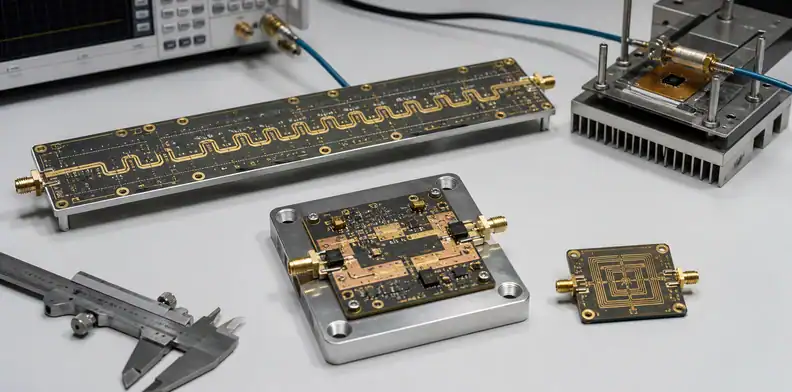
Quick Answer: Select RT/duroid 6002 when low TCDk, dimensional stability, and low moisture are central; select RT/duroid 6035HTC when the RF circuit needs much higher laminate thermal conductivity; and evaluate RT/duroid 6010.2LM when high Dk enables circuit miniaturization. These three Rogers materials solve different problems. Compare the exact thickness, copper, Dk/Df method, TCDk, thermal path, geometry, fabrication route, and model-to-coupon correlation before approving one.
An RT/duroid 6002 vs 6035HTC comparison is incomplete unless 6010.2LM is separated as a third architectural option. The first material emphasizes electrical and dimensional stability, the second adds a thermally conductive ceramic-filled system, and the third uses high Dk to reduce wavelength and circuit size. A designer can create a poor board by choosing the strongest headline property without checking the rest of the structure.
This article owns the three-way functional choice and does not repeat the low-Dk RT/duroid 5880 PCB page. The broader Rogers RO3000 family remains a separate topic. Those owner pages should be used when the design problem falls outside this 6002, 6035HTC, and 6010.2LM comparison.
Readers still choosing among general laminate classes should start with the PCB materials guide. This article begins after the project has already narrowed the decision to specialty Rogers RF materials.
Table of Contents
- Map the RF circuit to the property that controls it
- Use 6002 when stability protects phase and geometry
- Use 6035HTC when heat flow limits RF performance
- Use 6010.2LM when high Dk earns its penalties
- Compare Dk, TCDk, Df, and thermal data correctly
- Design thickness, copper, drilling, and bonding together
- Correlate the field model with production coupons
- Release a grade-specific RFQ and change plan
- Document the choice for production and future redesigns
Map the RF circuit to the property that controls it
Architecture rule: Identify whether phase stability, heat removal, or wavelength reduction is the primary constraint before comparing product values.
An antenna feed network may need phase consistency over temperature. A power-amplifier board may be limited by heat crossing the dielectric into a spreader. A compact filter, coupler, or matching network may benefit from a high-Dk material that shortens physical dimensions. Those are three different reasons to use a specialty laminate.
Write the circuit requirement before choosing a grade: frequency band, impedance, insertion loss, phase or resonance tolerance, power dissipation, heat-source footprint, temperature range, allowed board area, thickness, copper, surface finish, mounting, and qualification margin. Then rank the material properties by their effect on that design.
| Primary constraint | Candidate to evaluate first | Required confirmation |
|---|---|---|
| Phase/dimension stability | RT/duroid 6002 | TCDk, CTE, thickness, model correlation |
| Through-laminate heat flow | RT/duroid 6035HTC | Thermal path, copper, interface and temperature evidence |
| Circuit miniaturization | RT/duroid 6010.2LM | High-Dk geometry, tolerance, loss and fabrication |
The table is a starting point, not an automatic selection. A 6035HTC board still needs phase and loss checks. A 6010.2LM design still needs thermal and fabrication review. A 6002 design may require an external thermal solution.
Use 6002 when stability protects phase and geometry
Rogers’ high-frequency selector lists RT/duroid 6002 around Dk 2.94, Df 0.0012, and TCDk approximately +12 ppm/°C under the stated test conditions. The family is known for low moisture absorption and mechanical/electrical stability. Those characteristics can support microwave structures whose frequency or phase must remain predictable across fabrication and temperature.
Low TCDk does not eliminate all thermal drift. Copper dimensions, substrate expansion, connectors, components, solder joints, enclosure movement, and air dielectric regions also change. Use the material value inside a complete temperature model and define which finished-circuit measurement proves the requirement.
For phased arrays, delay networks, or narrowband filters, separate repeatability from absolute accuracy. A model can be tuned to one measured board, yet lot-to-lot or temperature variation may still move the response. Define whether the production requirement controls absolute phase, phase matching among channels, resonance, or drift over a temperature sweep. That distinction determines the coupon and sample size.
Dimensional stability matters when registration or artwork scaling affects coupled lines, filters, arrays, or multilayer alignment. Ask the fabricator how it controls material direction, panel compensation, imaging, and routing. A stable laminate cannot correct a poorly characterized production scale factor.
Choose the exact thickness and copper before completing the RF layout. Effective Dk and impedance depend on geometry, and the design value can differ from a process-specification number. Record the current Rogers TDS revision and the value used by the field solver.
Use 6035HTC when heat flow limits RF performance
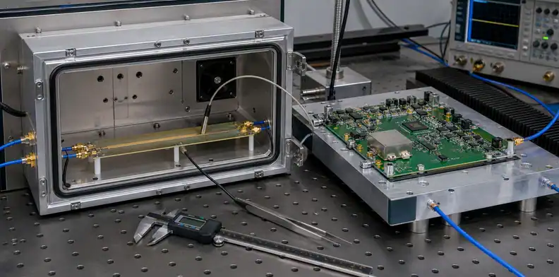
Thermal rule: Select 6035HTC only after a system thermal model shows that higher dielectric thermal conductivity improves the relevant junction-to-sink path.
Rogers positions RT/duroid 6035HTC as a high-thermal-conductivity, low-loss laminate. Its current product page and linked data sheet list process Dk 3.50 +/- 0.05 at 10 GHz using IPC-TM-650 2.5.5.5 clamped stripline, while the design Dk is 3.6 from an 8-40 GHz differential phase-length method. The same TDS lists thermal conductivity 1.44 W/m-K. These values can support RF power devices, amplifiers, bias networks, and other structures where heat must cross the substrate, but the project model must use the correct Dk type.
The laminate value is one element of a thermal resistance network. Copper spreading, via arrays, solder voids, component attachment, baseplate flatness, interface material, fasteners, enclosure, airflow, and heat-sink temperature can dominate. Compare junction temperature with the exact board construction rather than ranking laminates by W/m-K alone.
Check whether the design actually sends heat through the dielectric. If most heat leaves through a package ground pad and dense via field, copper and plating may control the result. If a microstrip device dissipates into the substrate and ground plane, laminate conductivity may have a larger role. Model both steady-state and transient conditions where the duty cycle matters.
The RF owner must also rerun impedance and phase using the 6035HTC construction. Higher thermal conductivity is not a drop-in property; ceramic loading, Dk, thickness availability, copper, drilling, and processing can change the circuit.
Review the assembly interface at the same time. A laminate improvement may be hidden by a thick or poorly controlled thermal interface layer, solder voiding, uneven clamping, or an undersized baseplate. State the interface material, bond-line or compression target, fastener pattern, flatness, and measurement boundary used in the thermal model. Then the first-article test can reproduce the model instead of measuring an unrelated fixture.
Use 6010.2LM when high Dk earns its penalties
RT/duroid 6010.2LM has a high dielectric constant, with Rogers selector data around process Dk 10.2 and design Dk 10.7 under the named methods, plus Df around 0.0023. The shorter wavelength can reduce resonator, filter, coupler, and antenna dimensions. That is the reason to consider it—not because a high Dk number is universally desirable.
High Dk concentrates fields and makes geometry, thickness, etch, and dielectric variation more influential. Trace dimensions can become narrow, coupling can change sharply, and connector or launch transitions may be harder to realize. The same physical tolerance can represent a larger electrical error in a compact resonant structure.
Miniaturization can also reduce power handling area and make thermal density more severe. Check conductor loss, dielectric loss, electric-field concentration, voltage stress, heat flow, and manufacturable line/space. A smaller circuit that requires impractical tolerances or creates a hot spot is not a successful optimization.
Use a tolerance analysis rather than a nominal model. Sweep Dk, substrate thickness, copper thickness, line width, gap, etch shape, and temperature. Identify which dimensions require tighter fabrication control and whether the supplier can measure them on the production panel.
High-Dk materials can also increase stored electric energy and alter radiation or coupling behavior. Check isolation between adjacent compact structures, edge clearance, ground-via placement, and the sensitivity of the launch. If the layout becomes too dependent on a dimension the fabricator cannot hold, increase circuit area or choose another architecture rather than placing an unrealistic tolerance on the drawing.
Compare Dk, TCDk, Df, and thermal data correctly
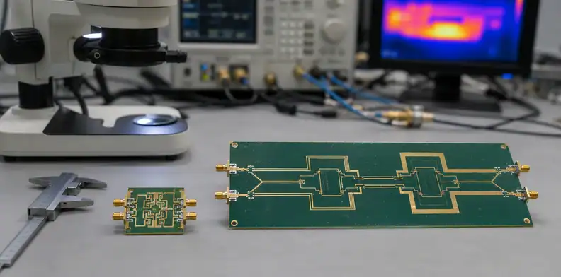
Data rule: Keep every value attached to its test method, frequency, direction, specimen, and revision; do not mix process and design Dk in one ranking.
Rogers often publishes more than one Dk because a material-specification method and a circuit-correlated design value serve different purposes. Df varies with method and frequency. TCDk describes how dielectric constant changes with temperature, while in-plane and through-thickness CTE describe physical expansion. Thermal conductivity measures heat transport, not temperature rise by itself.
Normalize the comparison:
| Field | 6002 question | 6035HTC question | 6010.2LM question |
|---|---|---|---|
| Dk | Which value drives phase? | Which value drives the RF geometry? | Process or design value for miniaturization? |
| Df | At what frequency/method? | Is conductor or dielectric loss dominant? | Does compact geometry raise total loss? |
| Temperature | TCDk and physical expansion | Property drift plus thermal gradient | Resonance sensitivity over temperature |
| Heat | External path sufficient? | Does 1.44 W/m-K change junction temperature? | Is power density acceptable after shrinking? |
Do not create contractual tolerances by copying typical values from a selector guide. Ask which properties are controlled by the material specification and which finished-circuit limits require coupons or assembly tests.
Design thickness, copper, drilling, and bonding together
The three families do not necessarily share the same thicknesses, copper options, panel availability, or fabrication route. Obtain current Rogers data and a fabricator-supported construction before layout release. Specify copper type, starting thickness, finished plating, foil profile, dielectric thickness, surface treatment, and any bonding material.
PTFE-based and ceramic-filled materials can require material-specific hole-wall preparation and handling. Use the PTFE PCB hole-wall preparation page to define evidence and approval fields, while relying on Rogers guidance and the qualified fabricator for the exact chemistry and process window. Do not prescribe a generic desmear recipe across all three grades.
Drill review should include tool wear, smear or debris removal, finished-hole tolerance, plating adhesion, aspect ratio, via fence density, backdrill, and microsection sampling. For 6035HTC, ask how ceramic loading affects tool life and hole quality. For 6010.2LM, verify that the compact geometry leaves manufacturable clearances around vias and pads.
| Fabrication feature | Supplier response required |
|---|---|
| Material preparation | Storage, cleaning, surface activation and handling route |
| Hole formation | Tool family, hit control, debris removal, inspection sample |
| Metallization | Hole-wall preparation, plating target and adhesion evidence |
| Bonding | Bonding material, press cycle, resin fill and thickness prediction |
| RF geometry | Etch compensation, measured dimensions and protected CAM zones |
Hybrid multilayers need explicit bond and CTE analysis. If the RF laminate is combined with FR-4 or another low-loss family, identify each interface, prepreg, press cycle, resin-fill need, copper balance, and dimensional-compensation plan. The high-frequency hybrid PCB stackup RFQ owns that mixed-material interface.
Correlate the field model with production coupons
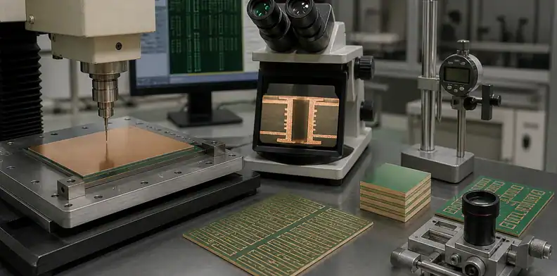
Proof rule: Validate the circuit quantity that drove the material choice—phase, thermal performance, or resonance—not merely a generic 50-ohm line.
For 6002, a phase or resonator coupon across temperature may be more meaningful than room-temperature impedance alone. For 6035HTC, combine RF coupons with a thermal vehicle that reproduces heat-source area, copper, vias, attachment, and boundary conditions. For 6010.2LM, use a resonant or dimensional structure sensitive to the high-Dk geometry and measure the features that drive its response.
All three grades still need traceable impedance and dimensional records. State coupon location, layer, copper, thickness, launch, calibration/de-embedding method, frequency range, limit, data format, lot identity, and disposition. A coupon built outside the same process region can give false confidence.
Correlate three records: the field-solver model, the as-built geometry, and the electrical result. If the coupon passes only after using an adjusted Dk, decide whether that value becomes the controlled production model and whether artwork needs revision. Do not leave the correction inside one engineer’s local simulation file.
Set a revalidation trigger for changes in material source, thickness, copper, bonding system, press route, drilling, plating, or critical geometry. The test plan can be narrower than the original qualification when the impact assessment proves which properties are affected.
Archive raw data as well as the pass/fail summary. Touchstone files, temperature logs, thermal images or sensor readings, dimensional measurements, and coupon photographs let engineering investigate drift later. A PDF that says “passed” cannot support model correlation after the material or process changes.
Release a grade-specific RFQ and change plan
The RFQ should name the exact RT/duroid grade and construction, not “Rogers high-frequency material.” Include native fabrication data, controlled drawing, layer map, stackup, RF geometry, model values, copper, drill/plating table, thermal drawing where relevant, coupon definitions, quantities, panel restrictions, acceptance rules, and approval owners.
Ask the supplier to return thickness and copper availability, manufacturing source, lead time, MOQ, proposed stackup, Dk/Df values used, geometry adjustments, fabrication route, qualification evidence, and exceptions. Require written approval before any alternate material, foil, bonding layer, or source enters production.
Use PCB material substitution approval when schedule, cost, or availability drives a proposal. A replacement for 6002 must preserve the stability need; a replacement for 6035HTC must preserve the thermal path; a replacement for 6010.2LM must reproduce the compact RF response. A generic low-loss comparison is insufficient.
Preserve the approved model, stackup, coupon result, thermal evidence, material certificate, and supplier exceptions for repeat orders. A complete fabrication package can be submitted to QueenEMS engineering for a grade-specific feasibility review.
Final choice: Buy the material whose complete production construction proves the controlling function, then protect that construction with grade-specific change control.
Document the choice for production and future redesigns
Record rule: Preserve why the grade was selected and which competing function was accepted as a tradeoff.
The material decision record should state the rejected alternatives as well as the selected grade. For 6002, explain the stability or phase requirement that outweighed a different thermal or size option. For 6035HTC, preserve the thermal model boundary and the measured improvement. For 6010.2LM, record the area reduction, critical tolerances, and RF correlation that justified high Dk.
Store the record with the schematic or RF specification, layout revision, solver files, stackup, and qualification data. Purchasing needs the exact order identity; fabrication engineering needs the process constraints; test engineering needs the coupon and fixture definition. A future redesign team needs to understand which property can change and which one cannot.
This record also prevents accidental cross-family reuse. A successful 6035HTC amplifier stackup is not evidence that 6035HTC should replace 6002 in a phase-sensitive network, and a compact 6010.2LM filter does not establish a high-Dk rule for every antenna feed. Reuse the decision method, not the conclusion.
FAQ
Is RT/duroid 6035HTC electrically better than 6002?
No universal ranking applies. 6035HTC targets higher thermal conductivity, while 6002 emphasizes low TCDk and stability. Compare the property that controls the circuit plus the resulting geometry and process.
Does 6010.2LM make every RF circuit smaller?
Its high Dk can shorten wavelength and reduce some structures, but launches, tolerances, coupling, loss, thermal density, and manufacturable line/space can limit the benefit.
Can one impedance coupon qualify all three materials?
No. The coupon should reproduce the selected material, thickness, copper, and process, and it must test the phase, thermal, resonant, or loss requirement that justified the grade.
What changes require a new review?
Review changes in grade, source, thickness, copper, bonding material, press route, drilling, plating, critical geometry, or test method. Revalidate the properties affected by the change.
Sources
- Rogers Corporation, RT/duroid laminates
- Rogers Corporation, high-frequency electronics product selector
Written by the QueenEMS Engineering Team
Upload your files today · Free DFM check before production · Ship worldwide
Get your PCB prototypes in as fast as 24 hours. We handle FR4, Rogers, and hybrid boards up to 40 layers in volume production, with advanced builds subject to engineering review — free prototypes for 2–4 layer FR-4 boards, no minimum order.
Just upload your Gerber + BOM — we source every part, assemble, and inspect (AOI + X‑Ray) so you don't have to chase suppliers. Boards ship in as fast as 24 hours.