
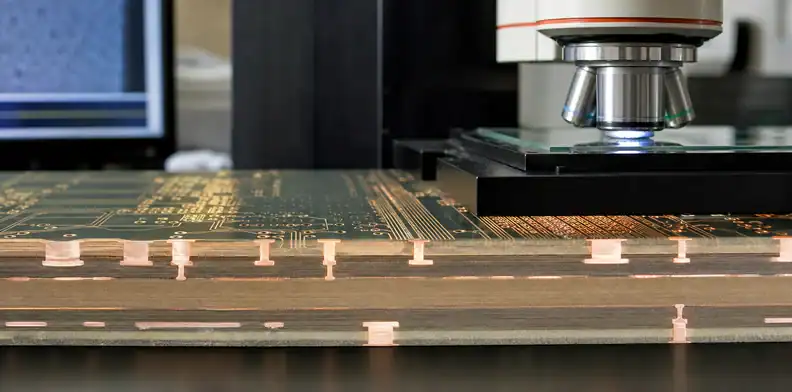
Quick Answer: PCB pattern plating changes the copper profile that the etch process must reproduce. A buyer should specify the finished line and space, copper target, controlled electrical features, and approval boundary for CAM compensation rather than assuming that the artwork width is the finished width. The supplier should return any local adjustment that changes the released geometry or the evidence used to prove it.
Pattern plating is one of the reasons a trace can be correctly drawn yet arrive at inspection with a different final shape. Copper grows in the exposed pattern, an etch-resistant deposit is applied, and the remaining copper is etched away. The result depends on the initial foil, the deposit, the resist opening, etch behavior, and the local copper pattern. That chain deserves its own review whenever line geometry controls impedance, clearance, current density, or assembly fit.
Table of Contents
- Use finished geometry as the acceptance target
- Understand how the pattern-plating route differs
- Separate compensation from an engineering change
- Review copper profile as well as width
- Control dense-to-open pattern transitions
- Link measurement to electrical intent
- Compare DFM proposals fairly
- Send a trace-geometry RFQ
- Set the right tolerance boundary
- Preserve evidence on revision changes
Use finished geometry as the acceptance target
The fabrication drawing should describe the feature that must exist after plating and etching, not just the nominal data shape. Finished line width, finished space, copper weight, layer position, impedance requirement, and allowed tolerance tell the supplier what must survive the route. CAD data remains the source of design intent, but a controlled board needs an agreed relationship between that data and the delivered copper.
For ordinary features, the fabricator may apply routine process compensation inside its agreed capability window. The line between routine and nonroutine moves when a narrow trace is part of a controlled transmission line, a safety clearance, a connector pad, or a high-current neck. A local change in those areas should be presented as a marked CAM question, not hidden in a generic DFM statement.
Geometry rule: judge pattern plating by the required finished conductor and clearance, not by the unprocessed artwork alone.
The PCB copper weight selection article provides the material context behind the finished-thickness callout. Where the affected trace also approaches a routed perimeter, include the copper-to-edge clearance requirement in the same DFM review so the two geometry limits are not approved separately.
Understand how the pattern-plating route differs
In a pattern-plated route, resist creates openings where additional copper is deposited. That added copper changes the profile of the conductor before the final etch. The etch step then removes unprotected copper and produces sidewall behavior that can affect the remaining trace width and spacing. A panel-plated route distributes copper differently, so a supplier should not use the same assumption for every outer layer without checking the design.
The buyer does not need to prescribe bath current, chemistry, or proprietary etch controls. The useful request is to identify whether the chosen route is suitable for the smallest feature and copper target, then to mark any alteration that changes the finished design rule. This creates a clear review point before the supplier spends time building an interpretation that engineering would reject.
| Route question | Why it matters to a buyer | Evidence that resolves it |
|---|---|---|
| Base foil and plated copper target | Sets the copper height that later etching must shape | Controlled stack-up and finished copper callout |
| Minimum line and space | Defines the narrowest usable image and etch margin | Supplier capability statement tied to the actual layer |
| Local dense pattern | Can alter deposit and etch loading | Marked DFM view or first-piece measurement |
| Critical electrical region | Limits what compensation may alter | Engineering-approved tolerance or CAM disposition |
Route boundary: a supplier may choose its qualified plating sequence, but it may not redefine the finished feature that the product requires.
Separate compensation from an engineering change
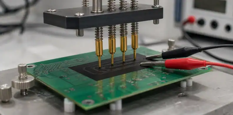
Compensation is used to account for known process behavior so that the delivered conductor meets the released requirement. It becomes an engineering change when it moves a controlled pad, alters a required clearance, changes an impedance width outside the permitted path, or introduces copper into a region where the design did not allow it. The phrase “etch compensation” should not be used to make either decision invisible.
Ask the supplier to show the affected layers and dimensions when the proposed adjustment reaches a critical area. A broad note that the factory will optimize artwork does not tell a purchaser whether two quotations represent the same finished board. A short, marked comparison is usually enough: original condition, proposed output, reason, and whether the design owner must approve it.
The AI PCB DRC versus fabrication capability article is useful when the original layout rule may not fit the selected process. This article deals with the next question: how the chosen fabrication route protects the approved geometry.
Change call: treat any compensation that crosses an electrical, spacing, or interface limit as an engineering approval item.
Review copper profile as well as width
A conductor can meet a width measurement at one location while still carrying an unfavorable sidewall profile, local neck, or residue condition elsewhere. The appropriate measurement method depends on the feature and the reason it is controlled. A high-current trace may need a copper cross-section; an impedance trace may need a finished width and dielectric context; a tight clearance may need an optical measurement at the actual narrow region.
Connect the inspection point to the failure mode. Measuring a wide coupon trace may not answer whether a dense connector escape remained open. Measuring only a surface width may not describe a plated profile where cross-section matters. The report needs the layer, feature, panel location, method, and acceptance disposition.
| Controlled condition | Weak evidence | Better evidence |
|---|---|---|
| Minimum clearance | One nominal CAM dimension | Measurement at the closest delivered gap |
| Impedance trace | Generic copper-weight statement | Finished geometry linked to the intended layer pair |
| High-current neck | Overall finished thickness | Cross-section or mapped copper condition at the narrow section |
| Fine-pitch pad escape | Panel-average result | Local optical check against released data |
Measurement check: choose evidence at the feature where the consequence occurs, not at the easiest place to measure.

Control dense-to-open pattern transitions
Dense copper regions and open fields can behave differently during plating and etching. A large open plane, a fine trace bank, a BGA fanout, and a copper-thieving area do not necessarily produce the same local deposit or etch burden. The supplier may use panel features to stabilize production, but those features need an approved boundary when they enter functional areas.
The copper thieving approval article explains why nonfunctional copper should be shown and reviewed. Pattern-plating review adds the finished-geometry question: whether a local production aid affects the features that must meet electrical or assembly limits.
An RF or high-speed area deserves a specific note when a small width change changes the design assumption. Conversely, an ordinary open area may allow normal manufacturing additions. Classifying those regions before quotation keeps CAM questions focused on the places that genuinely need engineering attention.
Locality rule: do not apply a panel-average process conclusion to a dense circuit area without a feature-specific check.
Link measurement to electrical intent
Trace geometry matters for different reasons. A differential pair may need stable impedance and symmetry; a power neck may need copper cross-section; a high-voltage gap may need preserved clearance; a card-edge feature may need pad position and width. One generic statement that the board meets line-and-space capability cannot close all of those decisions.
Put the design intent next to the selected features. The code-generated PCB impedance stackup review page provides the broader quote input for impedance layers. For pattern plating, add the practical question of whether copper growth and etch compensation can preserve the final conductor that the impedance model or current calculation used.
Where measurement is required, define whether the evidence is a coupon, a first-piece inspection, a microsection, or a calculated stack-up response. Each can be useful, but they should not be presented as interchangeable proof.
Electrical boundary: accept process compensation only when it preserves the design parameter that made the trace controlled.
Compare DFM proposals fairly
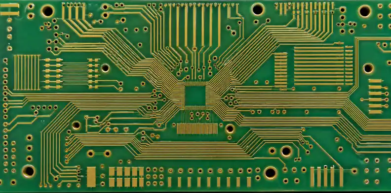
One supplier may offer a wider trace, another may request more clearance, and a third may accept the data with a tighter process route. Those responses do not have the same cost, schedule, electrical, or evidence consequence. Compare them in a short decision table rather than approving the first proposal that sounds manufacturable.
| Supplier response | Question for engineering | Purchasing implication |
|---|---|---|
| Routine compensation inside agreed limit | Does delivered geometry remain within the released tolerance? | Quote remains comparable |
| Wider or moved conductor | Does it change impedance, current, fit, or clearance? | Requires marked approval before PO |
| Different copper build | Does it change final profile or stack-up? | Compare material and process assumptions |
| Extra inspection request | Does it answer the actual controlled feature? | Add only if it closes a real risk |
Store the accepted mark-up with the design revision. A future reorder can otherwise inherit the altered production output while the original owner no longer remembers why it was accepted.
Comparison rule: choose between DFM proposals by their final electrical and mechanical effect, not by the shortest capability statement.
Send a trace-geometry RFQ
QueenEMS can review pattern-plating trace geometry when the package contains Gerber or ODB++ data, finished copper targets, minimum line and space by layer, stack-up, controlled-impedance or current notes, high-voltage clearances where relevant, and a marked map of areas that cannot accept geometry changes. Those inputs make the supplier’s compensation authority visible before the quote becomes a production baseline.
Request a response that states the proposed route, any local compensation that needs review, the expected evidence for the controlled feature, and the disposition owner for a CAM change. This lets a buyer compare offers without confusing a routine process adjustment with a redesign.
For a trace-geometry review, send the controlled layer data and finished-feature notes to QueenEMS through the manufacturing contact page. The response can identify whether the open point is a DRC margin, plating-and-etch effect, measurement gap, or an engineering change that belongs in the released drawing.
Set the right tolerance boundary
Tolerance language should identify the feature, finished state, and point where routine process adjustment becomes a disposition question. A global line-and-space claim is weak when a few locations control a connector interface, an impedance route, or a clearance path. Mark those areas and state whether the design accepts a range, an alternate construction, or no change.
| Tolerance statement | Product use | Open question it removes |
|---|---|---|
| Minimum finished line and space | General circuit survival | Whether a local controlled trace may move |
| Controlled width with layer pair | Electrical geometry | How the finished result will be checked |
| Named clearance | Mechanical or safety margin | Whether CAM can add copper nearby |
| Supplier capability claim | Process screening | The customer acceptance boundary |
Tolerance rule: the drawing should say where supplier freedom ends and engineering approval begins.
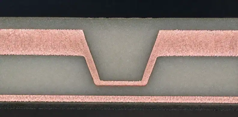
The evidence record should identify how the finished geometry was measured. Optical width measurement, coupon cross-section, electrical coupon data, and manual inspection do not answer the same question. For a controlled trace, record the applicable layer, the measured feature, the revision, and the accepted tolerance rather than filing an unlabelled image. A buyer can then distinguish a measurement that confirms the released line from one that only confirms that copper exists in the area.
For a line that affects impedance, the measurement plan also needs the reference condition that gives width its electrical meaning. Note the layer pair, dielectric construction, copper target, and whether the result is a dimensional check, an impedance result, or both. A width result by itself cannot close an impedance question when the surrounding construction has changed. Conversely, a coupon electrical result should not be used to excuse a visible clearance that falls outside the released drawing.
For high-current geometry, include the copper thickness and local neck width in the same record. A nominal top-view width can hide a plating profile that changes both resistance and thermal margin.
Preserve evidence on revision changes
A revised Gerber export can change a trace, copper pour, panel frame, or local density without changing the product name. Compare the revised output to the accepted DFM mark-up and measurement plan before a reorder. Equal layer count does not prove equal plating-and-etch conditions.
Use a short revision comparison that names the changed layers, minimum features, copper target, and adjacent density condition. A change to an unrelated silkscreen layer normally does not reopen a pattern-plating question; a revised copper island beside a narrow impedance trace might. This keeps the review proportional to the real process sensitivity.
Where a supplier changes panel format or proposes different thieving, compare the functional geometry before reusing the earlier evidence. The same board outline can present a different current distribution and etch burden when its production surroundings move.
Revision check: retain the approved finished-geometry interpretation with the fabrication data that produced it.

FAQ
Is pattern plating always used on outer layers?
No. Fabricators can use different qualified routes. The buyer’s concern is whether the chosen route can deliver the specified finished geometry.
Does etch compensation change the electrical design?
It should not when it stays within the approved finished requirement. A change that moves the electrical parameter or clearance outside that boundary needs engineering approval.
Can a coupon prove every fine trace on a panel?
No. A coupon is useful only when its construction and measurement represent the actual feature or an agreed worst-case condition.
Should copper thieving be shown to the design owner?
Yes, when it is proposed near functional copper or affects a controlled local geometry. Nonfunctional additions should not quietly enter an RF, high-speed, or high-voltage region.
Sources
- IPC-6012, Qualification and Performance Specification for Rigid Printed Boards
- EP1054081A2, printed-circuit metallization process
Written by the QueenEMS Engineering Team
Upload your files today · Free DFM check before production · Ship worldwide
Get your PCB prototypes in as fast as 24 hours. We handle FR4, Rogers, and hybrid boards up to 40 layers in volume production, with advanced builds subject to engineering review — free prototypes for 2–4 layer FR-4 boards, no minimum order.
Just upload your Gerber + BOM — we source every part, assemble, and inspect (AOI + X‑Ray) so you don't have to chase suppliers. Boards ship in as fast as 24 hours.