
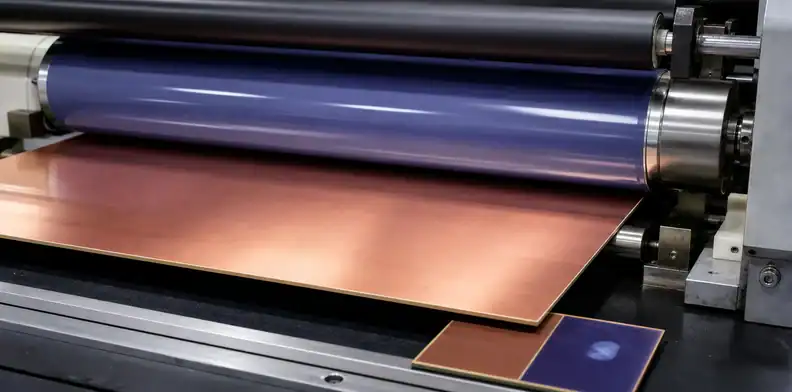
Quick Answer: PCB dry-film resist defects begin before exposure. Wrinkles, air voids, poor edge contact, particles, and uneven conformation can change the resist opening that later controls plating or etching. Buyers should connect fine-feature requirements to copper preparation, panel topography, film selection, inspection timing, and the supplier’s response when a defect appears.
The dry-film resist question is easy to overlook because the finished board does not show the film. Yet that temporary layer defines where copper remains, grows, or is removed. A quote for fine lines or dense pads is not complete until the supplier can explain how the panel’s actual copper surface will be prepared, laminated, imaged, developed, and inspected.
Table of Contents
- Locate dry film in the finished-copper chain
- Read wrinkles and voids as process evidence
- Match film conformation to copper topography
- Keep surface preparation visible
- Separate lamination findings from LDI findings
- Use pre-plate inspection before value is added
- Set a sensible containment path
- Prepare a fine-feature RFQ
- Compare the proposed route with the required feature
Locate dry film in the finished-copper chain
Dry film is a temporary image-forming material, but it affects permanent copper geometry. On an inner layer, the film protects the circuit that should remain during etching. On a pattern-plated outer layer, it also defines where copper and an etch-resistant metal build before the unwanted copper is removed. The same visible defect can have different consequences in those two routes.
Start with the feature that must survive the chain: a narrow trace, a close clearance, a BGA escape, a capture pad, or a controlled-impedance conductor. The fabrication data should identify the finished requirement, while the supplier decides how its qualified film, exposure, development, plating, and etching route will create it. A machinery name does not replace that connection.
The LDI imaging and registration article covers exposure placement and compensation. This page takes the earlier step: whether the resist arrives at imaging in a condition that can hold the intended pattern.
The later PCB etching process review helps explain why a marginal resist opening can become a finished-copper problem. For quote readiness, pair that process view with a DFM review before PO release when the layer contains near-limit line and space.
Copper texture belongs in the same discussion for fine features. The low-profile copper foil review helps separate a foil-selection question from a lamination defect, while still recognizing that surface topography affects film contact.
Process scope: dry-film review concerns the physical resist surface before imaging; LDI review concerns how the approved image is placed and developed.
Read wrinkles and voids as process evidence
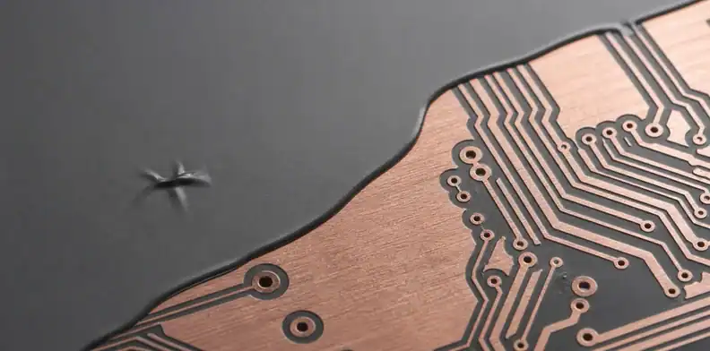
A wrinkle is not merely a cosmetic irregularity. It can move a resist edge, create an opening where copper should be protected, or prevent a developed image from matching the artwork. An air void can reduce local adhesion and become a weak point during development, plating, or etching. Repeated defects at the same panel position often point to a lamination contact or cleanliness issue rather than a random artwork error.
Ask the supplier to describe the location and shape of the finding. A long linear mark may suggest a roller or handling condition; isolated circular voids may point to particles or local surface features; failures near thick copper steps may show that the film did not conform to the topography. The buyer can evaluate the design consequence only after this distinction is visible.
| Finding before exposure | What may be affected later | Useful supplier record |
|---|---|---|
| Linear wrinkle | Shifted edge, open, or short after processing | Panel location and inspection photo |
| Local air void | Adhesion loss or unwanted opening | Feature proximity and containment decision |
| Edge lifting | Incomplete pattern protection near panel boundary | Whether the usable panel area is affected |
| Particle imprint | Local missing or distorted copper | Source-data comparison and defect disposition |
Defect call: a film finding is actionable when the report names its location relative to the released copper feature.
Match film conformation to copper topography
Flat copper and heavy, uneven copper do not present the same lamination surface. Dense plated areas, thick pads, copper coins, severe step transitions, and sharp local contours make it harder for a film to contact the panel uniformly. A fine-line request may be achievable on one area of a panel and unstable beside a high step if the process route was not qualified for that geometry.
The buyer need not set roller pressure or film temperature. It is enough to show the local topography in the Gerber data and drawing, call out the finished feature that cannot change, and require a marked response when the supplier sees insufficient process margin. This gives the fabricator room to use its qualified method without treating a design revision as an invisible process adjustment.
High copper is often discussed only as a current or thermal requirement. It also affects the image-transfer route. Pair this review with the copper plating distribution evidence page when the same outer layer combines thick plated copper and narrow circuit features.
Topography check: review film conformation wherever copper height and minimum spacing meet in the same local region.
Keep surface preparation visible
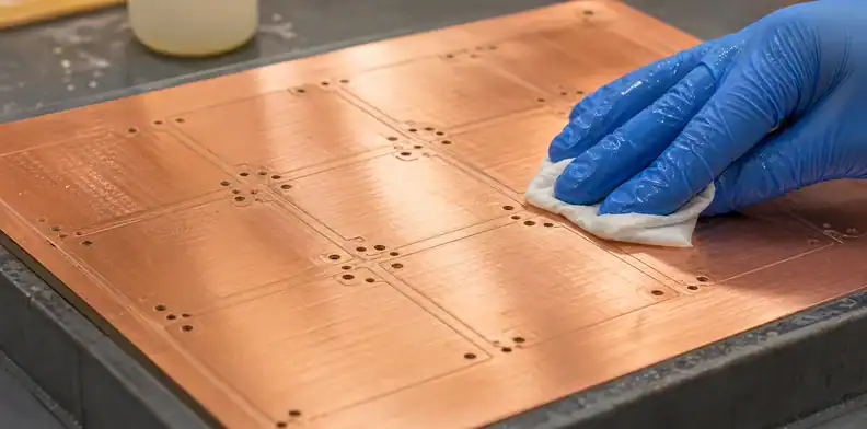
Dry film cannot adhere predictably to a surface carrying oxidation, fingerprints, drilling debris, residues, or uncontrolled handling marks. Surface preparation has to remove contaminants and create a suitable copper condition without altering a controlled thin foil or leaving chemistry that changes later imaging behavior. The qualified detail belongs to the fabricator; the acceptance question belongs to the released panel.
For an RFQ, identify unusual copper finishes, material combinations, reworked panels, or time-sensitive handling restrictions. A supplier should flag whether the selected imaging route is ordinary for that surface. That is more useful than a broad request for a “clean panel” because it tells the design owner whether a material or process condition needs review.
The process also has a timing side. Panels left waiting between surface preparation, film lamination, and imaging can face a different contamination or adhesion risk than panels processed inside the factory’s normal window. Buyers do not need a proprietary work instruction, but they can ask whether the planned build fits the standard qualified route.
| RFQ input | Why the fabricator needs it | Possible release question |
|---|---|---|
| Copper weight by layer | Determines local step height | Does the selected film route cover the topography? |
| Nonstandard laminate or coin | May change preparation compatibility | Is a separate material route needed? |
| Fine-line area map | Locates the smallest image margin | Does the supplier need a CAM discussion? |
| Rework or handling history | Reveals potential surface variation | Should the panel be remade rather than re-imaged? |
Surface boundary: accept a preparation explanation only when it supports the released material and finished-feature requirement.
Separate lamination findings from LDI findings
LDI can place an image accurately, but it cannot make a wrinkled or poorly adhered resist behave like a stable film. Conversely, a well-laminated film does not prove that the artwork revision, registration target, exposure, or development condition was correct. Combining all of these stages under the phrase “imaging issue” makes containment slow and can send the wrong team looking for the cause.
The supplier’s report should state the stage at which the first abnormal condition was observed: incoming copper, immediately after lamination, after exposure, after development, after plating, or after etch. That sequence matters because it separates a physical film contact problem from an image-data, registration, or downstream chemistry problem.
Where a pad or line is near its manufacturing limit, preserve the original film-stage evidence before a CAM correction is proposed. A later corrected panel may no longer show whether the first issue came from poor conformation, insufficient copper clearance, or an artwork condition outside the accepted margin.
Cause boundary: do not approve a permanent artwork change until the supplier identifies the process stage that first created the defect.
Use pre-plate inspection before value is added
The best time to catch a resist defect is before the panel receives expensive plating, etching, lamination, or finishing work. Depending on the route and risk, the supplier may use visual review, automated optical inspection, test patterns, or a first-piece approval. The buyer should ask which evidence is available for the controlled feature, not request every inspection record on the line.
For a product with one particularly dense region, a targeted first-piece image can be more useful than a generic statement that the whole panel passed. The reference revision, panel position, and defect disposition should appear in the record. That lets a later audit distinguish an accepted process signal from a board that simply moved forward without documented review.
Inner layers and outer layers should not be treated as identical evidence cases. Inner-layer defects can become inaccessible after lamination. Outer-layer defects may be associated with plated-hole or registration features that are visible only after different operations. The fabrication team should retain the inspection route and artwork revision that apply to the layer being reviewed.
Inspection point: place the check before the next irreversible operation and tie it to the artwork revision that was actually processed.
Set a sensible containment path
When a lamination defect appears, the first action is to establish scope. Identify the panel, layer, side, film lot or work order reference where available, affected feature type, and whether the finding is isolated or repeated. That record lets the supplier decide whether to stop one panel, inspect a related set, or revisit the lamination equipment without making unsupported claims about the root cause.
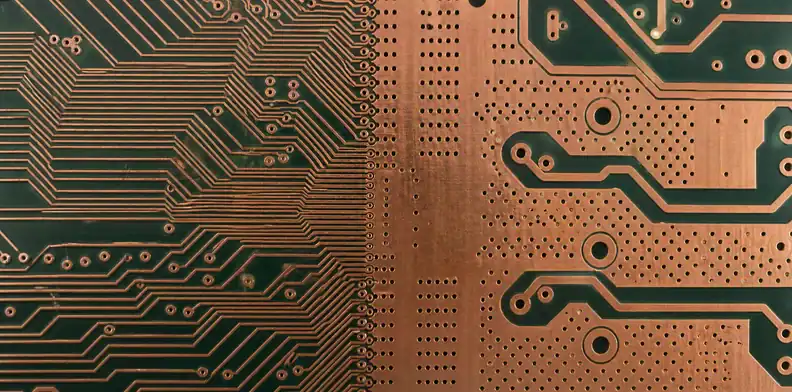
Containment should also protect the design. A supplier may offer a wider trace, larger clearance, changed copper pattern, or alternative process. Those are not equivalent remedies. A local film defect may call for process correction; a recurring margin problem may show that the design needs a controlled change. Engineering should receive a mark-up before any edit that moves a functional copper feature.
At incoming inspection, a buyer rarely sees the original film. The useful preventive record is the final decision: whether the issue was contained, whether the released design changed, and whether first-lot evidence is needed on the next revision. That makes a repeat order easier to review without pretending that a finished-board photo proves every earlier process condition.
Containment rule: correct the process when the design remains inside margin; escalate to engineering only when the proposed cure changes released geometry or construction.
Prepare a fine-feature RFQ
For dry-film risk, provide the released layer artwork or ODB++ job together with copper weights, minimum finished line and space, a marked view of dense or stepped areas, stack-up, required impedance or pad geometry, and known material restrictions. The aim is to identify the image-transfer questions before a supplier has priced the work under an assumed process route.
Ask the supplier to respond with the relevant feature limit, any local risk from copper topography or surface condition, proposed evidence for a first lot, and a marked question for any geometry change. That response is far more useful than a broad capability statement because it lets purchasing compare the same feature and evidence request across quotations.
For a focused image-transfer and CAM review, send the critical layer views and finished-feature notes to QueenEMS through the fabrication contact page. The review can identify whether the issue belongs to film conformation, imaging registration, plating/etch geometry, or a design margin that needs approval before production.
Compare the proposed route with the required feature
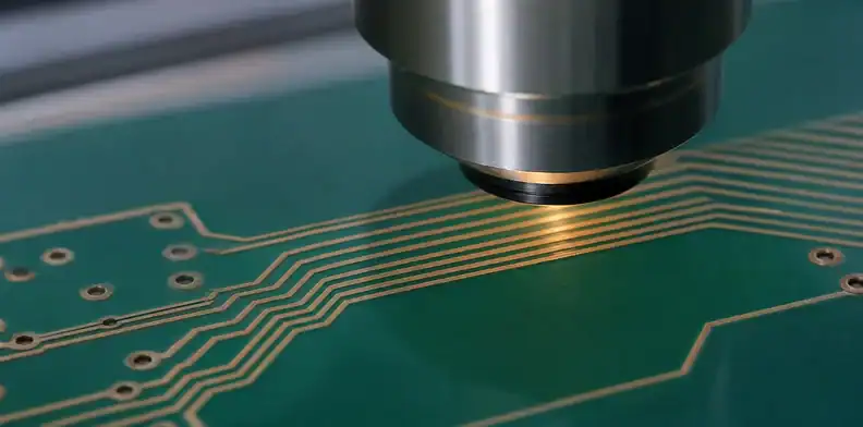
Fine-line capability should be tested against the whole image-transfer route, not accepted from a nominal equipment claim. A supplier may have an LDI platform suitable for small features yet need a different film family, panel format, copper plan, or inspection approach when the same feature sits beside heavy copper or a local height transition. The practical question is whether the proposed route preserves the released feature after development, plating, and etch.
| Feature condition | Review question | Approval outcome |
|---|---|---|
| Narrow line in a flat area | Does the qualified film and image route meet the finished width? | Proceed with normal DFM confirmation |
| Narrow space beside thick copper | Can film contact and later etch retain the clearance? | Request a local process or CAM response |
| Dense BGA escape region | Are pads, clearances, and adjacent mask relationships all represented? | Confirm the finished-feature interpretation |
| Controlled trace near a copper step | Does the route preserve geometry used for impedance intent? | Engineering reviews any proposed change |
The table also prevents an unhelpful argument about where the problem “belongs.” The fabricator can own the qualified process route, while the design owner decides whether a different finished geometry is acceptable. Both decisions are needed when the requested feature sits near the available manufacturing margin.
A sensible containment response also preserves the panel state long enough to identify the stage of loss. A wrinkle found before exposure calls for film and lamination review; a distorted line found after plating may require comparison with the developed image, deposit profile, and etch result. Stripping and restarting can be appropriate for a recoverable panel, but it should not erase the observation that determines whether the next panel needs a different setup. Record the affected layer, panel area, feature type, and point in the route where the condition was first seen.
Route check: release the fine feature only after the supplier names the process path and the boundary for any geometry change.
FAQ
Can LDI remove a dry-film wrinkle risk?
No. LDI controls exposure placement; it cannot restore physical contact or adhesion where the resist film is wrinkled, voided, or lifted.
Does every fine-line board need special dry-film evidence?
No. Evidence should match the risk. A routine qualified feature may need no special record, while a local high-step or near-limit area can justify first-piece confirmation.
Is a surface-cleaning note enough for approval?
No. The note needs to connect the prepared surface to the actual copper weight, material condition, and finished feature the supplier is being asked to process.
Should a supplier change the artwork to fix a repeated defect?
Only after the defect stage and design margin are understood. A process issue should not automatically become a permanent geometry change.
Sources
Written by the QueenEMS Engineering Team
Upload your files today · Free DFM check before production · Ship worldwide
Get your PCB prototypes in as fast as 24 hours. We handle FR4, Rogers, and hybrid boards up to 40 layers in volume production, with advanced builds subject to engineering review — free prototypes for 2–4 layer FR-4 boards, no minimum order.
Just upload your Gerber + BOM — we source every part, assemble, and inspect (AOI + X‑Ray) so you don't have to chase suppliers. Boards ship in as fast as 24 hours.