
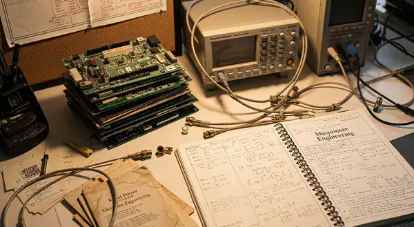
The RF Challenge
In RF Design, Every Micron Decides Between Success and Scrap
Signal interference, impedance drift, and suppliers who don't understand RF layout rules cost you redesign cycles, missed certifications, and scrapped prototypes. The real question is: does your PCB manufacturer actually speak RF?
What Derails RF Projects
- Signal interference from poorly controlled trace geometry — causing insertion loss 2–3× higher than simulation predictions
- Impedance tolerance exceeding ±10% because your supplier lacks TDR verification and uses nominal Dk values instead of measured ones
- Suppliers unfamiliar with RF layout PCB rules: incorrect ground via fencing, improper microstrip-to-stripline transitions, and inadequate copper pour isolation
- 4–6 week lead times because the factory doesn't stock Rogers or Taconic laminates and treats your RF board like a standard FR-4 job
How Queen EMS Eliminates These Risks
- RF-trained engineers review every design for signal integrity before fabrication — catching layout issues that cause interference, not discovering them after assembly
- Impedance control within ±5% on every RF PCB, verified by TDR coupon testing on every production panel — documented report ships with your boards
- 20+ years manufacturing RF PCBs means we understand ground plane management, via fencing patterns, and transition structures as well as your design team does
- Rogers 4350B, 4003C, RT/duroid 5880, and Taconic TLY permanently in stock — your prototypes enter production immediately, not after weeks of material procurement
Stop losing prototypes to suppliers who don't understand RF. Get an expert assessment.
Request Free RF DFM ReviewRF Manufacturing Services
Complete RF PCB Manufacturing & Microwave PCB Assembly
Three specialized service lines covering the full RF development cycle — from bare board fabrication through assembled and tested microwave modules, all under one roof.
High-Precision RF PCB Fabrication
Our production lines are built specifically for RF PCB manufacturing on PTFE, ceramic-filled, and thermoset hydrocarbon substrates. Laser direct imaging (LDI) delivers 0.05mm trace width accuracy, while real-time etch compensation maintains the dimensional precision that keeps your RF circuits performing exactly as simulated — from 500 MHz through 77 GHz.
Microwave PCB Assembly
RF-sensitive components demand assembly expertise that general SMT lines cannot provide. Our microwave PCB assembly process uses nitrogen reflow profiling calibrated for Rogers substrates, precision paste deposition for fine-pitch RF ICs, and post-reflow X-ray verification on every BGA and QFN — ensuring your amplifiers, filters, and mixers perform to specification from the first board.
Hybrid PCB Stack-up Engineering
Combining Rogers or Taconic on RF signal layers with FR-4 on power and digital layers cuts material costs by up to 40% without sacrificing insertion loss on critical paths. Our lamination engineers manage CTE mismatch, resin flow, and registration accuracy across dissimilar materials — delivering hybrid PCBs that survive thermal cycling from −40°C to +125°C without delamination.
Need RF fabrication, assembly, or both? Our team designs the optimal workflow for your project.
Discuss Your RF RequirementsMaterial Selection Guide
The Expert's Guide to Rogers RF PCB & PTFE Materials
In RF antenna PCB design, substrate selection directly controls antenna radiation efficiency, thermal stability, and insertion loss. The wrong Dk/Df specification turns a working simulation into a failed prototype. This reference covers the materials we stock and process daily — mapped to real-world frequency bands and application requirements.
| Material | Dk (10 GHz) | Df (10 GHz) | Optimal Frequency | Best RF Applications | Cost |
|---|---|---|---|---|---|
| Rogers RO4350B | 3.48 ± 0.05 | 0.0037 | Up to 10 GHz | RF power amplifiers, GPS antennas, 5G base station front-ends | $$ |
| Rogers RO4003C | 3.38 ± 0.05 | 0.0027 | Up to 18 GHz | LNA modules, RF switches, cellular infrastructure, microwave filters | $$ |
| Rogers RT/duroid 5880 | 2.20 ± 0.02 | 0.0009 | Up to 77 GHz | Automotive radar (24/77 GHz), satellite LNB, mmWave antenna arrays | $$$ |
| Taconic TLY-5 | 2.20 ± 0.02 | 0.0009 | Up to 40 GHz | Military phased-array radar, precision test fixtures, microwave couplers | $$$ |
| PTFE / Teflon PCB | 2.10 – 2.55 | 0.0008 – 0.0015 | Up to 60 GHz | Broadband couplers, stripline filters, waveguide transitions, RF sensor boards | $$–$$$ |
| FR-4 (Reference) | 4.2 – 4.7 | 0.018 – 0.025 | Below 1 GHz | Digital control logic, power distribution — not recommended for RF signal layers | $ |
All materials stocked in-house. Hybrid stack-ups (Rogers RF PCB layers + FR-4 digital layers) available for cost-optimized designs.
Unsure which Rogers RF PCB material matches your frequency band and loss budget?
Get Expert Material RecommendationProject Portfolio
RF PCB Products Built in Our Factory
Real RF projects delivered to global clients — each manufactured with full impedance control documentation, cross-section analysis, and on-time shipment.
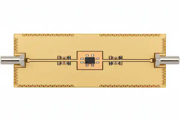
RF Power Amplifier PCB
- Material Rogers RO4350B
- Layers 4L
- Frequency 2.4 – 6 GHz
- Surface Finish ENIG
- Impedance 50Ω ± 5%
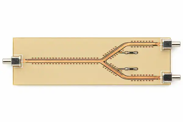
Microwave Power Splitter
- Material Rogers RO4003C
- Layers 6L
- Frequency DC – 18 GHz
- Surface Finish Immersion Silver
- Impedance 50Ω ± 5%
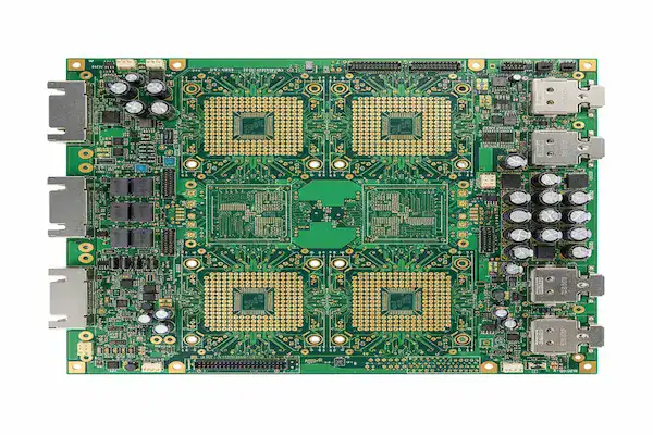
5G Base Station Communication PCB
- Material Rogers 4350B + FR-4 Hybrid
- Layers 8L Hybrid
- Frequency 3.5 GHz / 24.5 – 29.5 GHz
- Surface Finish ENIG
- Impedance 50Ω ± 5%
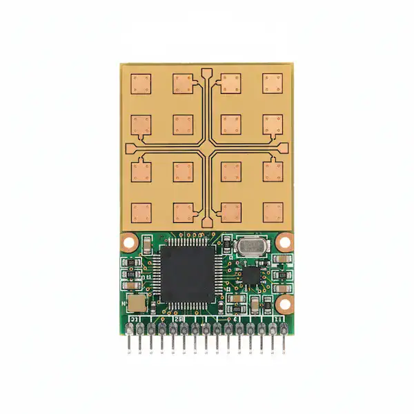
77 GHz mmWave Radar RF Board
- Material RT/duroid 5880
- Layers 4L
- Frequency 76 – 81 GHz
- Surface Finish Immersion Silver
- Impedance 50Ω ± 5%
Have a similar RF project? Upload your files for a tailored manufacturing plan.
Get Your RF Project QuoteProcess Deep-Dive
Mastering RF PCB Manufacturing Process Control
Standard PCB factories treat RF boards like any other job. We don't. These four specialized process controls are the reason our RF PCBs measure within spec on first-article — not after three revision rounds.
Plasma Desmear for PTFE
PTFE and Rogers substrates resist standard chemical desmear. Our plasma treatment removes drill smear residue at the molecular level — ensuring clean via walls that maintain signal continuity across layers. Without this step, plating adhesion fails and via reliability drops below acceptable RF thresholds.
Laser Direct Imaging (LDI)
RF microstrip lines demand trace accuracy to ±0.5 mil — conventional photolithography cannot deliver this consistently. Our LDI system writes circuit patterns directly to the photoresist with laser precision, eliminating film distortion errors that cause impedance deviation on every board in the panel.
Solder Mask Thickness Control
On RF circuits, solder mask acts as an additional dielectric layer that shifts effective impedance. We control mask thickness to ±10 μm and use low-Dk solder mask formulations specifically selected for RF applications — preventing the 3–5% impedance shift that standard mask materials introduce on microstrip transmission lines.
Real-Time Etch Compensation
Copper etching is never perfectly isotropic — without compensation, final trace widths differ from design by 0.3–0.8 mil. Our automated etch-factor feedback loop measures copper removal in real time and adjusts exposure parameters per-panel, delivering the trace geometry accuracy that keeps your RF circuits within their impedance corridor.
Want to see how these RF process controls apply to your specific design?
Request Process Capability ReviewEngineering Partnership
RF Design Support & Quick-Turn Prototyping
We're not just an RF PCB manufacturer — we're your signal integrity partner. Our engineering team reviews your RF layout PCB design for manufacturability before a single panel enters production.

From RF Layout Review to First-Article in Days, Not Months
Every RF project begins with a dedicated engineer reviewing your Gerber files, stack-up specification, and impedance targets. We identify potential signal integrity risks — ground plane discontinuities, via stub resonances, inadequate clearance around RF traces — before they become expensive prototype failures.
Our quick-turn RF prototyping lane delivers finished boards in as few as 5 working days using in-stock Rogers and Taconic materials. Each prototype ships with a complete impedance test report and cross-section analysis, giving your design team the data needed to validate performance immediately.
- Free RF DFM review with every quote — catching layout issues before fabrication
- Quick-turn prototyping: 5–10 working days from approved files to shipped boards
- Impedance report + cross-section analysis included with every prototype shipment
- Dedicated RF engineer assigned to your project throughout the entire build cycle
- Seamless transition from prototype to production — identical process parameters, zero re-qualification
Upload your RF design files and receive expert DFM feedback within 2 hours.
Submit Files for RF ReviewIndustry Applications
Where Our RF & Microwave PCBs Perform
From satellite transponders orbiting at 36,000 km to automotive radar modules operating at highway speeds — our RF PCBs deliver reliable signal integrity in the world's most demanding environments.

Satellite Communication
LNB converters, Ku/Ka-band transponders, and space-qualified RF front-ends requiring ultra-low insertion loss and thermal cycling stability from −55°C to +125°C.

Aerospace & Defense
Military phased-array radar, electronic warfare systems, and avionics RF modules built to IPC Class 3 standards with full material traceability and lot documentation.

Automotive mmWave Radar
24 GHz and 77 GHz ADAS collision-avoidance modules, blind-spot detection sensors, and autonomous driving radar arrays demanding automotive-grade reliability.

5G Infrastructure
Massive MIMO antenna arrays, small-cell RF front-end modules, and base station power amplifier boards operating across sub-6 GHz and mmWave frequency bands.
Working in a specialized RF application? We adapt our process to your industry's exact requirements.
Discuss Your ApplicationWhy Queen EMS
Your Competitive Advantage in RF PCB Manufacturing
Three capabilities that separate a specialized RF PCB manufacturer from a general-purpose factory — and directly reduce your project risk, development cost, and time to market.
20-Year RF Engineering Veterans
Our RF engineers have completed over 2,000 high-frequency PCB designs across radar, satellite, and 5G applications. They review your stack-up, recommend optimal materials for your specific frequency band, and identify impedance risks before fabrication — turning potential redesigns into first-pass successes that save you weeks and thousands in development costs.
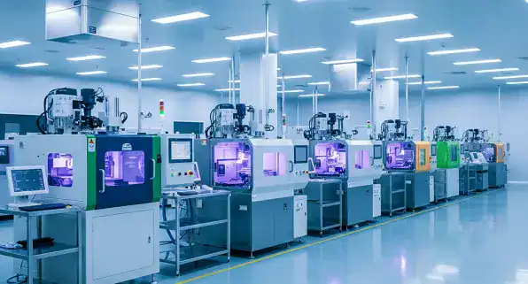
100+ Imported Production Systems
Our factory floor runs dedicated RF production lines equipped with LDI exposure, plasma desmear, TDR impedance testing, and nitrogen-atmosphere reflow systems. These aren't shared with standard FR-4 production — they're calibrated exclusively for PTFE, Rogers, and Taconic substrates, delivering the process consistency that RF circuits demand across every board in your order.

2-Hour Technical Quote Response
Submit your RF design files and receive a detailed engineering assessment within 2 hours during business days. Our quote includes material recommendations, impedance feasibility analysis, and a realistic production timeline — not a generic price sheet. You make informed decisions immediately, keeping your development schedule on track without waiting days for supplier feedback.
Experience what working with a dedicated RF PCB manufacturer actually feels like.
Get Your Free RF Engineering ReviewDirect Factory Supply for Global Innovation
Located in the heart of China's manufacturing hub, Queen EMS provides complete, transparent, and scalable RF manufacturing capabilities.
100+ Advanced Machines
We process every step in-house using cutting-edge equipment. This direct control eliminates middleman delays, ensuring your high-frequency production stays strictly on schedule while reducing overall project costs.
Dedicated RF SMT Workshop
Our facility includes an isolated, mature SMT line tailored for microwave assemblies. This strict environmental separation prevents cross-contamination, protecting the delicate signal integrity of your layout.
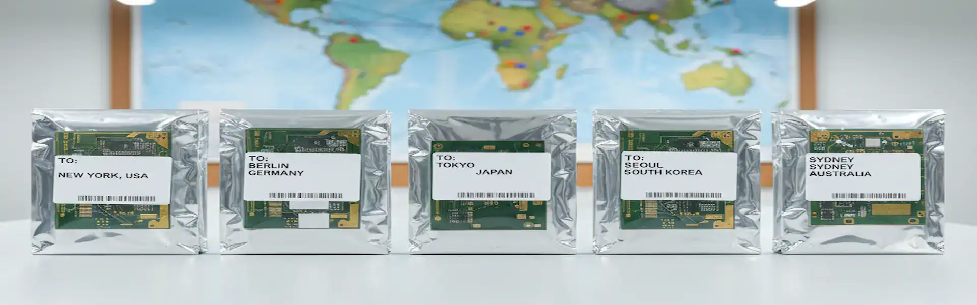
20+ Years Export Expertise
We have smoothly delivered highly complex boards to the USA and Europe for two decades. Our team completely understands international compliance, meaning you enjoy risk-free sourcing and fluent technical communication.
Looking for a direct factory that understands RF standards?
Schedule a Virtual Factory TourZero Compromise on RF Quality Assurance
High-frequency performance requires absolute precision. Our rigorous inspection systems guarantee your specifications are met before shipment.
Real-Time TDR Testing
We verify every production batch using advanced Time Domain Reflectometry testing. This precise measurement guarantees your impedance control remains strictly within the ±5% tolerance, ensuring flawless signal propagation.
100% AOI & X-Ray Inspection
We deploy automated optical inspection and deep X-ray scanning on all inner layers and microvias. This detects micro-defects instantly, preventing hidden shorts or opens from reaching your final microwave assembly.
Ionic Cleanliness Control
A rigorous ionic contamination test is performed prior to any surface finish. By removing all chemical residues, we eliminate the risk of parasitic capacitance and surface leakage under high-frequency operation.
Don't let poor inspection ruin your RF design.
Get Your Guaranteed Quality BoardUltimate Protection & Logistics
RF components and special finishes are highly sensitive. We protect your investment from our factory floor directly to your hands.
Military-Grade Vacuum Sealing
Every board is tightly sealed in an oxygen-free vacuum environment immediately after final inspection. This strictly prevents moisture absorption and pad oxidation, maintaining perfect solderability for your SMT process.
Premium ESD Shielding
For PCBA projects, we enclose all units in high-grade anti-static shielding bags. This completely blocks electrostatic discharge during transit, ensuring your costly RF amplifiers and filters arrive 100% functional.
Reinforced Global Cartons
We utilize thickened, crash-proof outer cartons combined with global logistics partners like DHL and FedEx. Your high-precision boards are insulated against physical shocks, arriving safely at your facility within 3-5 days.
We care about your boards just as much as you do.
Review Our Shipping StandardsRF & Microwave PCB Manufacturing FAQ
Answers to the questions RF engineers ask most before choosing a high-frequency PCB fabrication partner.
Over 40% of RF PCB projects we receive arrive specifying Rogers RO4350B by default — even when the actual operating frequency would perform equally well on lower-cost RO4003C. That material choice alone adds 25–35% to board cost with zero performance benefit. Our engineers flag these over-spec situations during DFM review and recommend optimized alternatives — last quarter, this saved three customers a combined $18,000 in unnecessary material premiums. Upload your design and we'll run a free material optimization check.
What RF and microwave PCB materials do you stock?
How tight is your impedance control on RF PCBs?
Can you handle hybrid stack-ups mixing Rogers and FR-4?
What's the typical lead time for RF PCB prototypes?
How do you prevent impedance drift between prototype and production batches?
Have a high-frequency design that needs precision fabrication? Let's review your requirements.
Upload Your RF PCB FilesPartner with a Trusted RF PCB Manufacturer Today
Upload your Gerber files now to receive a free, expert DFM review and a precise quotation within 2 hours.