
Quick Answer: PCB delamination is the physical separation of laminate layers, often appearing as visible blisters or internal voids. It occurs when internal vapor pressure exceeds the material’s bond strength during reflow (260°C peak). You must reject any batch showing more than 1% blistering, as internal separation reduces long-term reliability by 50% or more.
Key takeaways:
- Diagnosis: Fabrication faults show clean separation; assembly faults show charred resin or browning.
- Material Choice: Standard FR4 (Tg 130°C) is insufficient for lead-free reflow; demand High-Tg (Tg >170°C).
- Prevention: Baking boards at 105°C for 4–6 hours eliminates 95% of moisture-induced “popcorning.”
- Testing: Demand the IPC-TM-650 2.4.24 thermal stress test (288°C for 10s) to verify material bond strength.
Table of Contents
- 1. What Is PCB Delamination and Why Does It Matter?
- 2. How Do You Identify Delamination — What Does It Look Like Inside and Outside?
- 3. What Causes PCB Delamination at the Fabrication Stage?
- 4. What Causes PCB Delamination During Assembly and Reflow?
- 5. How Do You Diagnose Whether Delamination Came From Fab or Assembly?
- 6. What Role Does Moisture Sensitivity Level (MSL) Play in Delamination?
- 7. How Can You Prevent Delamination Through Material and Process Choices?
- 8. What Should You Do When You Find Delamination in Production Boards?
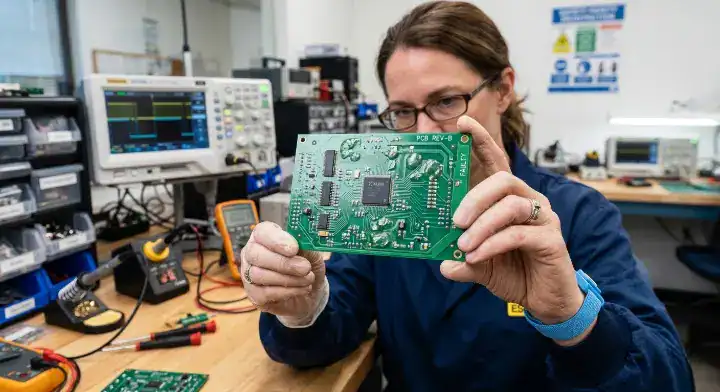
Finding bubbles on a board after reflow is more than a cosmetic defect; it is a structural failure. While many suppliers blame “excessive heat,” the truth often lies in trapped moisture or poor lamination during the pcb fabrication defects prevention phase. At QueenEMS, we maintain a 99.7% first-pass yield by strictly controlling humidity and material baking before the first component ever touches the board. We treat every pcb bubbling incident as a data point for a total process audit.
1. What Is PCB Delamination and Why Does It Matter?
PCB delamination is the separation of internal layers—typically between copper foil and prepreg or prepreg and the core—resulting in physical gaps that trap air or moisture. This defect matters because it creates high-impedance paths, destroys signal integrity, and causes catastrophic failure when internal copper traces fracture under thermal stress.
Here is the reality: A board with delamination is a ticking time bomb.
- It reduces heat dissipation by up to 40% as air gaps act as thermal insulators.
- It exposes internal copper to oxidation and ionic contamination.
- It causes intermittent opens in high-density vias during temperature fluctuations.
Bottom line: Treat any signs of blistering as a total batch failure; there is no reliable way to “repair” a delaminated board once the internal layers have separated.
2. How Do You Identify Delamination — What Does It Look Like Inside and Outside?
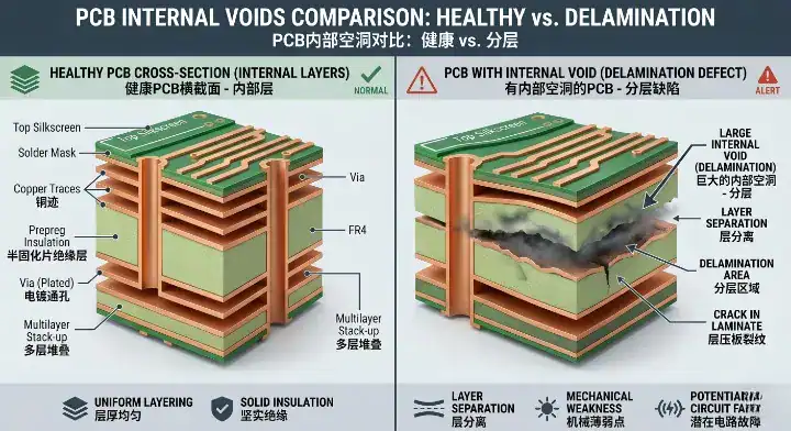
Visual pcb blistering causes are the most obvious signs, appearing as raised white or silver patches on the board surface, often near large copper planes or high-heat components. However, internal delamination is invisible to the naked eye and requires ultrasonic scanning (C-SAM) or cross-section microscopy to detect voids between the inner laminate layers.
- Visual Inspection: Look for “mealing” or white spots under the solder mask.
- Cross-Sectioning: Costs $200–$400 and provides 100x magnification of the layer stack-up.
- C-SAM (Acoustic Microscopy): The only non-destructive way to map 100% of internal air gaps.
| Detection Method | Can Detect | Typical Cost | When to Use |
|---|---|---|---|
| Visual Inspection | Surface blisters, discoloration | Free | Every board at AOI |
| X-Ray | Large copper shifts, shorts | $50 – $150 | Verifying BGA joints |
| C-SAM / SAT | Internal air gaps, voids | $500 – $1,500 | High-reliability/Medical batches |
| Cross-Section | Precise layer separation distance | $200 – $400 | Root cause diagnosis (Destructive) |
Choose visual inspection for quick filtering of gross defects, but choose cross-sectioning if you need legal proof of a supplier’s manufacturing failure.
Bottom line: Don’t rely on X-rays alone; X-rays pass through air gaps, making them nearly useless for detecting vertical layer separation.
3. What Causes PCB Delamination at the Fabrication Stage?
At the fabrication stage, pcb delamination causes center on insufficient resin curing or contamination of the inner copper layers before the lamination press. If the prepreg absorbs moisture in the PCB factory’s storage area before bonding, that moisture becomes permanently trapped, only to vaporize and expand during your 260°C reflow process.
- Contamination: Fingerprints or oil on inner layers prevent the resin from bonding to copper.
- Inadequate Curing: Incorrect temperature/pressure cycles leave the resin in a “B-stage” state.
- Moisture Absorption: Poor factory humidity control (exceeding 50% RH) during lay-up.
Bottom line: If the delamination is localized to the board edges, it usually points to poor lamination pressure; if it is centralized, it points to trapped moisture during fabrication.
4. What Causes PCB Delamination During Assembly and Reflow?
During assembly, the primary driver of delamination is the “popcorn effect,” where moisture trapped inside the PCB rapidly turns to steam at 217°C–260°C, creating internal pressure that exceeds the material’s bond strength. This is aggravated by multiple reflow cycles (top and bottom side) or an improperly tuned reflow soldering profile optimization that applies excessive dwell time above the material’s Tg.
Look at the math: Water expands roughly 1,600 times its volume when turning into steam. In a 0.062″ board, even a microscopic amount of moisture creates enough PSI to tear the resin away from the copper foil.
- Thermal Shock: Entering the reflow oven too quickly without a proper preheat zone.
- Multiple Cycles: Each subsequent reflow weakens the chemical bonds of the resin.
- Manual Rework: Localized high heat from soldering irons can cause instant blistering.
Bottom line: Most assembly-level delamination is avoidable through pre-assembly baking and strict adherence to moisture sensitivity protocols.
5. How Do You Diagnose Whether Delamination Came From Fab or Assembly?
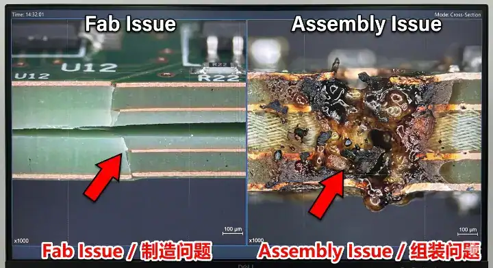
To diagnose the source, you must perform a cross-section analysis: fabrication-origin delamination shows clean, smooth separation between layers with no charring, while assembly-origin delamination often shows resin browning or carbonization due to excessive heat. Fabrication issues are usually batch-wide, whereas assembly issues correlate with specific moisture exposure or rework events.
Factory Case Study: A client called us in panic—they had 800 finished boards showing visible blistering on the bottom-side ground plane. Their PCB supplier insisted the boards were fine. We cross-sectioned 6 sample boards. Under the microscope, all 6 showed clean separation between the prepreg and copper foil with no thermal degradation marks—no charring, no browning. This was a fabrication failure caused by contaminated copper foil. We confirmed this by taking 10 unused boards from the same batch and running a thermal stress test (288°C for 10s); 7 of 10 failed. The client recovered $32,000 in costs after we provided this evidence.
| Symptom | Probable Source | Verification Method | Who Fixes |
|---|---|---|---|
| Clean separation, no browning | Fabrication | Thermal Stress Test (Unused board) | PCB Factory |
| Charred resin, browning | Assembly | Review Reflow Profile Data | SMT House |
| Blisters only near BGAs | Moisture (Popcorning) | Bake Test vs. Non-Bake Test | SMT House |
| Edge-only separation | Fabrication | Cross-section pressure check | PCB Factory |
Choose a third-party lab for diagnosis if your CM and PCB factory reach a deadlock, as the cross-section data is indisputable.
Bottom line: Never accept “it’s the oven’s fault” without a cross-section showing resin charring; if the resin is clear, the factory failed the lamination process.
6. What Role Does Moisture Sensitivity Level (MSL) Play in Delamination?
While MSL is usually associated with components, PCBs themselves have a specific floor life, and extended exposure to humidity before soldering creates the perfect conditions for popcorn-induced delamination. JEDEC J-STD-033 defines moisture sensitivity for components, but the same physics applies to the laminate material: the more moisture the board absorbs, the lower its “time to delamination” (T260/T288) becomes.
Factory Case Study: An industrial client shipped PCBs to us that had been in their warehouse for 11 months. We noticed a slight tackiness on the solder mask. We recommended baking at 105°C for 6 hours. The client refused. We ran a test: 50 boards unbaked, 50 boards baked. The unbaked batch had a 14% delamination rate (blisters near large planes). The baked batch: 0% delamination. The client immediately approved baking for the rest of the shipment.
| MSL / Storage Type | Floor Life | Baking Schedule | Recommended Storage |
|---|---|---|---|
| Sealed Vacuum Bag | 12 Months | None required | <30°C / 60% RH |
| Exposed < 48 hours | 2 Days | None required | Dry Cabinet (<10% RH) |
| Exposed > 72 hours | Expired | 105°C – 125°C for 4-6 hours | Dry Cabinet |
| Solder Mask Tackiness | Critical | 125°C for 8 hours | Immediate Production |
You can find more details on preventing these moisture-related issues in our guide on moisture sensitivity level prevent popcorning.
Bottom line: If your boards have been out of vacuum packaging for more than 72 hours in a non-controlled environment, you must bake them before reflow.
7. How Can You Prevent Delamination Through Material and Process Choices?
The most effective pcb delamination prevention is choosing materials with a high decomposition temperature (Td) and a glass transition temperature (Tg) that exceeds your peak reflow temperature by at least 50°C. For lead-free processes (260°C peak), standard FR4 with a Tg of 130°C is highly susceptible; you should demand High-Tg FR4 (Tg >170°C).
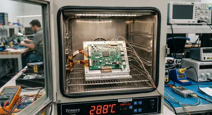
IPC-TM-650 method 2.4.24 specifies the thermal stress test for PCB materials, exposing samples to 288°C molten solder. Materials passing this test demonstrate the bond strength required for modern production. You should also ensure your stack-up is balanced to prevent pcb warping causes which can put mechanical stress on internal layers.
| Material Grade | Tg (Glass Transition) | Td (Decomposition) | Lead-Free Compatible? |
|---|---|---|---|
| Standard FR4 | 130°C – 140°C | 300°C | No (High Risk) |
| Mid-Tg FR4 | 150°C | 325°C | Marginal |
| High-Tg FR4 | 170°C – 180°C | 350°C | Yes (Recommended) |
| Polyimide | 250°C+ | 400°C+ | Yes (Aerospace) |
Choose High-Tg materials for any 4+ layer board going through lead-free reflow, as the cost increase (typically 10-15%) is far cheaper than scrapping a production run. You can compare different FR4 material Tg grades here.
Bottom line: Don’t save $1 on laminate to risk $100 in assembly scrap; specify Tg170 or higher for all lead-free projects.
8. What Should You Do When You Find Delamination in Production Boards?
When you find delamination, you must immediately halt production, isolate the affected batch, and run a thermal stress test on unpopulated boards from the same lot to determine if the issue is material-based. If the raw boards pass the 288°C stress test, the problem likely lies in your assembly house’s storage conditions or reflow profile.
- Quarantine: Stop the SMT line immediately to prevent further loss.
- Material Verification: Send 5 unused boards for IPC-TM-650 testing.
- Traceability Check: Check if the delamination is confined to one lot number or one fabrication date.
- Contract Negotiation: If the raw boards fail the stress test, the PCB supplier is liable for all assembly and component costs.
Bottom line: Speed is critical; the longer you wait to diagnose, the harder it is to prove whether the moisture was absorbed at the factory or in your own warehouse.
FAQ
What is PCB delamination? PCB delamination is the separation of internal layers (copper from resin or resin from resin) within a circuit board. It is caused by internal vapor pressure from trapped moisture expanding during high-temperature reflow. It results in visible blisters or internal voids that fracture copper traces.
How do I know if the PCB factory or the SMT house is at fault? Perform a cross-section analysis. If the resin is clean and clear at the separation point, it is usually a fabrication fault (poor lamination). If the resin is charred or brown, it is an assembly fault (excessive heat). You should also run a thermal stress test on an unused board to verify the material quality.
Can I fix a board with delamination? No, delamination is a permanent structural failure of the internal laminate bonds. While some suggest “clamping and heating,” this does not restore the chemical bond between layers and will lead to trace fractures or impedance failures later. You must scrap and replace the board.
Does baking PCBs prevent delamination? Yes, baking PCBs at 105°C for 4–6 hours removes absorbed moisture, preventing the “popcorn effect” during reflow. It is highly recommended for boards that have been out of vacuum packaging for more than 72 hours. Baking is a low-cost insurance policy against 90% of assembly-level delamination.
What is the best material to prevent delamination? High-Tg FR4 (Tg > 170°C) with a high decomposition temperature (Td > 340°C) is the industry standard for preventing delamination in lead-free processes. These materials maintain their bond strength much better at the 260°C peak temperatures required for modern soldering.
Finding pcb bubbling after production doesn’t have to be a mystery. You need a partner who understands the chemistry of the laminate as well as the physics of the oven.
At QueenEMS, we offer Free DFM/DFA engineering reviews to ensure your material choices match your thermal requirements. We utilize up to 60-layer PCB fabrication capabilities and perform 100% 3D AOI and X-Ray inspection on every joint. From prototype to mass production, we provide the turnkey transparency you need to eliminate field failures. Stop guessing about root causes. Contact us at QueenEMS to build a reliable, delamination-free future for your hardware.
Written by the QueenEMS Engineering Team.
Upload your files today · Free DFM check before production · Ship worldwide
Get your PCB prototypes in as fast as 24 hours. We handle FR4, Rogers, and Flex up to 60 layers — free prototypes for 2–4 layer boards, no minimum order.
Just upload your Gerber + BOM — we source every part, assemble, and inspect (AOI + X‑Ray) so you don't have to chase suppliers. Boards ship in as fast as 24 hours.