
Reliable Multilayer PCB Manufacturer | Claim Free 2-4L Prototypes
From standard 4-layer boards to complex 32-layer HDI designs, QueenEMS delivers high-precision fabrication for your demanding applications. Ready to test our service quality? New B2B partners can upload Gerber files today to claim a FREE 2-4 layer standard FR4 prototype. Get factory-direct pricing and engineering support for your next build.
- Quick-Turn Prototypes in 3-5 Days
- Free Stack-up & DFM Engineering Check
- One-Stop In-House PCB Assembly (PCBA)
- ISO 9001 & UL Certified Production
Claim Free Prototypes
Response within 2 hours by our engineers.
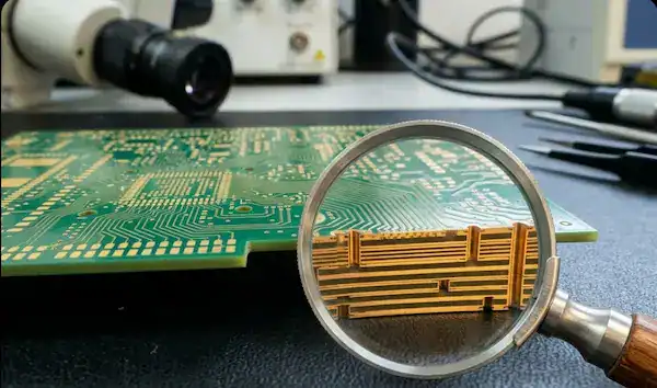
Overcoming Critical Sourcing Hurdles
Signal Integrity Issues
High-speed designs demand strict routing tolerances. We utilize sub-mil impedance control protocols to prevent signal loss, ensuring your final device operates flawlessly without interference.
Thermal Mismanagement
Intense heat loads can lead to premature board delamination. Our advanced lamination process with high Tg materials guarantees long-term structural reliability even in extreme operational environments.
Supply Chain Latency
Unpredictable delivery windows disrupt assembly lines. Our 24-hour quoting system and streamlined workflow keep your projects strictly on schedule, eliminating costly downtime.
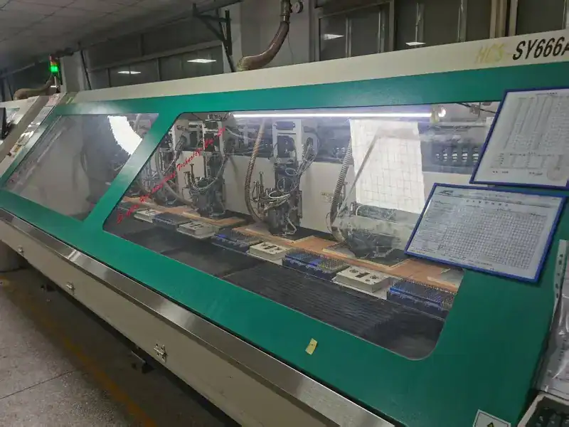
Comprehensive Multilayer PCB Fabrication Services
Quick-Turn Prototyping
Powered by dedicated rapid-response engineering lines. Receive your complex multilayer samples in just 3-5 days, empowering you to iterate faster and beat competitors to market.
Scalable Mass Production
Driven by fully automated manufacturing facilities. Maintain precise and consistent quality from 100 to 100,000 units, effectively driving down your per-unit cost safely.
Complimentary DFM Check
Supported by a comprehensive Design for Manufacturability review. We identify and resolve potential fabrication errors before production, saving your budget from expensive rework.
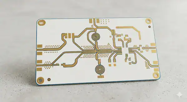
Specialized Multilayer Board Solutions
High-Density Interconnect (HDI)
Built with micro-vias and blind/buried structures. Maximizes routing density in constrained spaces, allowing you to create smaller, lighter, and smarter electronic products.
High-Frequency Boards
Manufactured using premium Rogers and Teflon substrates. Minimizes signal attenuation at high frequencies, delivering peak performance for your 5G and radar applications.
Heavy Copper Power Boards
Fabricated with up to 10oz internal copper layers. Provides superior current-carrying capacity and heat dissipation, ensuring your power modules run cool and stable.
Turnkey PCB Assembly (PCBA) Services
Beyond bare board fabrication, we offer complete in-house assembly. We combine China’s manufacturing efficiency with international-level process control to provide stable, high-reliability electronic assemblies.
Advanced SMT & THT
Equipped with mature Surface Mount Technology (SMT) and mixed-technology (THT) capabilities. We seamlessly handle low- to mid-volume production runs with extreme precision and speed.
Strict Quality Testing
We guarantee performance by utilizing automated optical inspection (AOI), X-Ray for hidden joints, and customized functional testing to ensure a 100% yield rate before your products ship.
Engineering-Driven Execution
Say goodbye to slow replies and unclear technical explanations. Our sales and engineering teams work closely together to ensure fast quotations and consistent execution for your assembly needs.
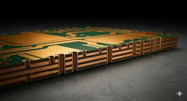
The Engineering Behind Perfect Stack-Ups
Impedance Optimization
Involves precise calculation of dielectric thickness and copper weight. Achieves exact impedance matching for PCIe interfaces, safeguarding your high-speed data transmission.
Electromagnetic Compatibility
Relies on the strategic arrangement of signal and ground planes. Drastically reduces cross-talk and EMI, ensuring your product passes stringent certification tests easily.
Structural Integrity
Requires symmetrical layer construction and resin flow management. Prevents board warping during high-temperature assembly, increasing the yield rate of your PCBA process.
Advanced Multilayer PCB Manufacturing Specifications
Base Materials
- Standard FR4 (Tg 130-180)
- High Frequency Rogers, Teflon
- Thermal Metal Core (Al/Cu)
- Flexible Polyimide (PI)
We stock premium laminates from industry-leading brands, giving you the exact dielectric properties needed to maintain signal integrity in demanding multilayer PCB design layouts.
Precision Tolerances
- Min Line/Space 3 mil / 3 mil
- Min Hole Size 0.15mm (Mechanical)
- Impedance Control ±5% (Standard ±10%)
- Layer Registration ±2 mil
Our state-of-the-art LDI (Laser Direct Imaging) equipment pushes the limits of trace precision, allowing you to successfully route high-density components like BGAs without short circuits.
Surface Finishes
- Gold ENIG, Hard Gold
- Silver/Tin Immersion Ag / Sn
- Lead-Free HASL LF, OSP
- Specialty ENEPIG
Select from a full spectrum of RoHS-compliant finishes. Our perfectly flat ENIG coating provides excellent oxidation resistance, guaranteeing flawless solder joint reliability during PCBA.
Inside Our Multilayer PCB Fabrication Process
Brown Oxide Treatment
We apply a micro-roughened chemical coating to inner copper layers. This vastly increases the surface area for the prepreg to grip onto, preventing catastrophic delamination during high-temperature reflow.
Vacuum Lamination
Multiple layers are fused using heavy hydraulic presses under strict vacuum conditions. This extracts all trapped air bubbles, ensuring uniform dielectric thickness and robust structural integrity across the board.
Plasma Desmear
Drilling generates heat that smears resin over inner copper connections. We utilize advanced plasma etching to completely remove this smear, guaranteeing flawless electrical conductivity through your vias.
Standard & Expedited Lead Times
Reliable delivery schedules tailored to your project's layer count and volume requirements.
| Layer Count | Volume (sq.m) | Time (Days) | Expedited (Hours) |
|---|---|---|---|
| Double-sided (2L) | < 1 | 5 | 15 |
| 1 ~ 5 | 7 | ||
| > 5 | 8 | ||
| 4 Layers | < 1 | 5 | 24 |
| 1 ~ 5 | 7 | ||
| > 5 | 12 | ||
| 6 - 8 Layers | < 1 | 6 | 36 |
| 1 ~ 5 | 9 | ||
| > 5 | 12 | ||
| 10 Layers | < 1 | 10 | 60 |
| 1 ~ 5 | 10 | ||
| > 5 | 15 | ||
| > 10 Layers | < 1 | 10 | 72 |
| 1 ~ 5 | 10 | ||
| > 5 | 15 |
Why Top Engineers Choose QueenEMS as Their Supplier
±5% Impedance Control
While the industry standard is 10%, our specialized pressing algorithms tighten tolerances to 5%. This eliminates signal reflection, giving your RF and high-speed data products unparalleled stability.
100% AOI & Flying Probe
Every inner and outer layer passes through automated optical and electrical testing. We catch opens and shorts before shipping, ensuring you never assemble a defective bare board.
A-Grade Core Materials
We absolutely refuse to use recycled substrates. By exclusively utilizing A-grade FR4 and high Tg materials, your PCBs gain exceptional mechanical strength and heat dissipation capabilities.
Buyer's Guide: Evaluating Multilayer PCB Reliability
Not all boards are created equal. As your trusted multilayer PCB manufacturer, we encourage you to check these critical metrics when qualifying any factory.
Hole Wall Copper Thickness
Hidden voids inside vias cause intermittent failures in the field. We provide detailed micro-section reports proving a minimum 20µm copper plating in the barrel, guaranteeing your connections survive thermal cycling.
Residues left from etching can trigger dendrite growth and short circuits (CAF). Our automated chemical washing lines meet strict IPC-TM-650 standards, keeping your sensitive electronics safe from corrosion over their lifespan.
Even a slight offset in inner layers can cause drills to break annular rings. We use real-time X-Ray target drilling equipment to ensure perfect concentricity across all layers, completely eliminating via breakout risks.
In-House Manufacturing Power
We do not outsource. By keeping all fabrication processes strictly in-house, we maintain absolute control over quality, intellectual property, and your delivery timeline.
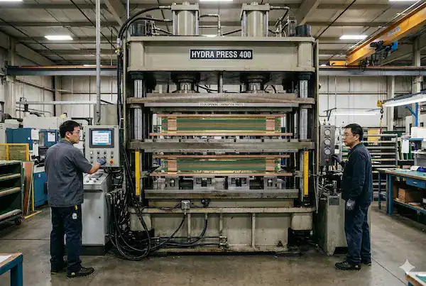
Massive 4-story hot presses apply precise temperature and pressure profiles. This ensures flawless resin flow and bonding across highly complex 32-layer assemblies.
Equipped with laser-guided routing and drilling tools. We accurately drill micro-vias down to 0.15mm, providing the foundation for ultra-compact HDI routing spaces.
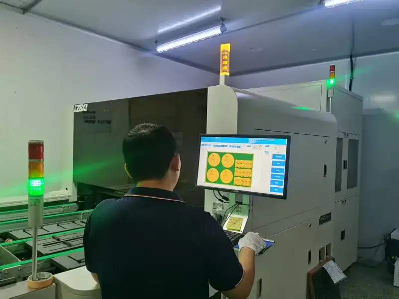
High-resolution cameras instantly compare your etched copper against original Gerber files. This guarantees 100% trace fidelity before the board moves to the next stage.
Zero-Defect Multilayer PCB Production
100% Electrical Testing
Every single board undergoes strict Flying Probe or Bed-of-Nails testing. We identify any potential open or short circuits early, ensuring you never waste time or components assembling a defective bare board.
Inner Layer X-Ray Inspection
High-resolution X-ray scans verify the internal alignment of your high-layer-count boards. This guarantees perfect via-to-pad registration, preventing hidden connectivity failures in complex blind/buried via designs.
Automated Optical Inspection
Advanced AOI systems continuously scan etched copper traces against your original Gerber files. This catches micro-defects like pinholes or narrowed traces, maintaining maximum reliability across your entire batch.
Secure Packaging & Global Express Delivery
Vacuum & Anti-Static Sealing
Every multilayer board is vacuum-sealed with desiccant and packed in ESD-safe bags. This completely seals out moisture and static electricity, keeping your bare boards perfectly ready for immediate SMT assembly upon arrival.
3-5 Days Global Shipping
Through strategic partnerships with DHL, FedEx, and UPS, we offer priority air freight. Enjoy reliable 3 to 5-day door-to-door global delivery that meets your tightest production deadlines effortlessly.
Proactive Order Tracking
Our online portal provides real-time tracking updates from fabrication line to final delivery. Gain full supply chain visibility, eliminating uncertainty and allowing you to schedule your assembly lines with confidence.
Trusted by 500+ Innovative Electronics Brands
Finding a reliable multilayer PCB supplier was our biggest challenge until we found QueenEMS. Their impedance control is flawless, and the 8-layer prototype arrived in Germany in just 4 days. Exceptional engineering support!
QueenEMS acts like an extension of our own team. Their free DFM check saved us from a costly blind-via mistake on a 12-layer HDI board layout. Their communication is miles ahead of typical trading companies.
We transitioned our mass production of multilayer circuit boards to QueenEMS last year. The consistency across batches is incredible, and the pricing is fully transparent. A highly recommended manufacturing partner.
Frequently Asked Questions
We provide clear, direct answers tailored to the unique concerns of purchasing managers, hardware engineers, and business owners.
What is your Minimum Order Quantity (MOQ) for multilayer boards?
How do you maintain competitive pricing while using A-grade materials?
What are your limits for HDI routing, trace/space, and via sizes?
How do you guarantee the ±5% impedance control mentioned?
Can you handle the transition from quick-turn prototypes to full turnkey PCBA?
What is the standard lead time for 8+ layer circuit boards?
How do you ensure the protection of our Intellectual Property (IP)?
Are you a direct factory or a trading company, and why does it matter?
Ready to Accelerate Your PCB Project?
Send us your Gerber files today. Our engineers will provide a free DFM check and a highly competitive quote within 2 hours.