
Common Challenges in
HDI PCB Manufacturing
HDI fabrication isn't just "smaller holes and finer traces" — it's a fundamentally different process chain where every step requires precision that conventional PCB manufacturing was never designed to achieve. Most factories talk HDI capability but deliver inconsistent results when complexity scales beyond basic 1+N+1 structures.
Microvia Drilling Precision Instability
Laser drilling a 0.1mm via requires micron-level positional accuracy and consistent beam energy. Most factories struggle to maintain tight tolerances across an entire panel — resulting in via diameter variation, incomplete drilling, and connection reliability issues that only surface during thermal cycling or electrical testing.
Laser Drill Quality Batch Variation
Your first HDI prototype may pass perfectly. The problem appears at volume: laser optics degrade, focus drifts, and process parameters that worked for batch one produce rejects in batch five. Without real-time monitoring and frequent calibration, yield collapses — and you only discover it after assembly and functional test failures.
Sequential Lamination Registration Offset
Every lamination cycle introduces thermal expansion and mechanical stress. Achieving sub-mil layer-to-layer registration across 3+ lamination passes demands tooling precision and material science expertise most multilayer shops simply don't have — leading to buried via misalignment and connection opens that kill entire panels.
Fine Line Width/Spacing Production Drift
Etching 2 mil traces requires perfect photoresist adhesion, controlled chemical concentration, and stable temperature — factors that drift throughout a production day. A factory claiming 2/2 mil capability in their spec sheet often can't deliver it consistently across 100 panels without significant rework or scrap rates.
Need a factory that treats HDI manufacturing as engineering, not just equipment operation?
Discuss Your HDI PCB RequirementsWhy Many PCB Factories Struggle
with True HDI Production
Owning laser drill equipment doesn't make a factory an HDI manufacturer any more than owning a CNC machine makes someone a precision machinist. Real HDI capability is built on process control depth, material science knowledge, and the engineering discipline to maintain micron-level tolerances across thousands of panels — not just the first prototype batch.
Equipment Without Process Expertise
Many multilayer shops purchase laser drilling systems to enter the HDI market but lack the process engineering depth to optimize beam parameters, drilling strategy, and via fill electroplating. The result: equipment sits underutilized, or worse, produces unreliable vias that pass visual inspection but fail under electrical stress or thermal cycling. HDI isn't a capital investment problem — it's a knowledge problem.
Surface HDI vs. True Sequential Build-Up
A 1+N+1 structure with microvias only on outer layers is "HDI-lite" — technically HDI, but it doesn't solve the routing density challenges of complex designs. True HDI requires managing 2+N+2 or even ELIC (Every Layer Interconnect) structures with stacked and staggered microvias across multiple sequential lamination cycles. Most factories stop at simple build-ups because they can't control registration or yield at higher complexity.
Inconsistent Batch-to-Batch Quality Control
Your prototype run succeeds because the factory assigns their best technician and watches every parameter. Production runs fail because process control isn't automated, documented, or enforced. Laser focus drift, lamination pressure variation, and plating bath contamination introduce defects that accumulate across batches. Without statistical process control and real-time monitoring, HDI "capability" becomes HDI "sometimes we get it right."
No Engineering Support for Stack-Up Optimization
A conventional multilayer shop takes your Gerber files and builds them as-is. An HDI manufacturer reviews your stack-up before quoting — identifying impedance control issues, thermal management risks, and via structure optimizations that prevent failures before the first panel is drilled. Factories that lack in-house RF and signal integrity knowledge can't guide HDI designs toward manufacturability — they just build what you send and hope.
Want to work with a factory that engineers HDI processes, not just operates HDI equipment?
Talk to Our HDI Engineering TeamThe Hidden Risks of Poor
HDI Stack-Up Design
An HDI stack-up isn't just a layer count and via structure — it's a system-level decision that affects signal integrity, thermal performance, mechanical reliability, and manufacturing yield. Stack-up mistakes made early in design become expensive failures late in production, often surfacing only after assembly when rework is prohibitively costly.
 Complex Stack-Up Analysis
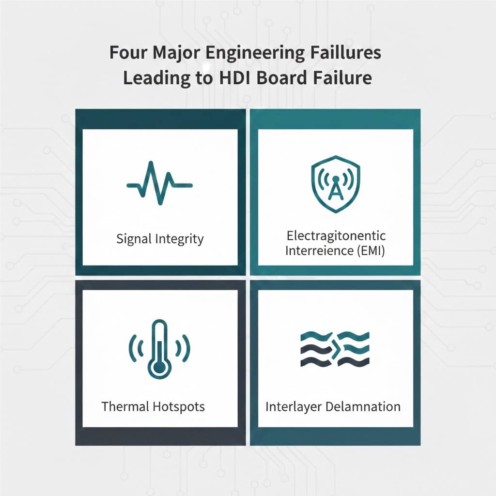
Four Engineering Failures That Kill HDI Boards
Stack-up design isn't optional optimization — it's foundational. When done poorly, the board may physically assemble but fail functionally in ways that are difficult or impossible to diagnose without destructive analysis.
- Signal Integrity Degradation: Inadequate ground plane separation or incorrect dielectric selection causes impedance discontinuities, reflection, and crosstalk — problems that only appear at speed during real-world operation, not during bring-up testing.
- EMI Susceptibility and Emission: Without proper layer stacking strategy — return path management, shielding layer placement — high-speed signals radiate interference or pick up noise from adjacent circuitry, failing EMC compliance testing after PCB fabrication is complete.
- Thermal Hotspot Formation: Thin dielectric layers improve electrical performance but reduce thermal conductivity. Without thermal vias and copper balancing, power-dissipating components create localized hotspots that accelerate material degradation and reduce MTBF.
- Lamination Failure Under Stress: Mismatched CTE (coefficient of thermal expansion) between core and build-up materials causes delamination during thermal cycling — a failure mode invisible until the board experiences real operating temperature swings in the field.
EMC Test Failures
Radiated emissions exceed limits after full assembly complete
Thermal Runaway Risk
Components overheat due to inadequate heat dissipation paths
Signal Integrity Issues
High-speed interfaces fail bit error rate specs under load
Field Delamination
Layers separate after thermal cycling in actual use conditions
Unsure if your HDI stack-up design will survive real-world operating conditions? We review stack-ups before fabrication — not after failures.
Request a Stack-Up Design ReviewWhat Defines True
HDI Printed Circuit Boards
"HDI" has become a marketing term diluted by loose application. True HDI technology is defined by specific structural features and fabrication processes that conventional multilayer manufacturing fundamentally cannot achieve. Understanding these distinctions determines whether your board design gets the capability it actually requires.
Microvias (≤0.15mm)
Laser-drilled vias with diameters at or below 150 microns — typically 0.1mm in production. Unlike mechanically drilled vias, microvias connect only adjacent layers, enabling high-density routing between sequential build-up layers without consuming valuable routing channels across the entire board stack.
Blind & Buried Vias
Blind vias connect outer layers to internal layers without traversing the full board thickness. Buried vias connect internal layers only. Both structures free up routing space and reduce parasitic capacitance compared to through-hole vias — critical for high-speed differential pairs and dense BGA fanouts.
Sequential Lamination
Building the PCB in stages — core lamination, first build-up, second build-up — rather than a single lamination cycle. Each stage adds routing layers and microvias, enabling complex interconnect structures (1+N+1, 2+N+2, ELIC) impossible with conventional multilayer processes.
Fine Line Technology (≤75µm)
Trace widths and spacing at 3 mil (75µm) or finer, achieved through advanced imaging, precise etching chemistry, and tight process control. Fine line capability is what allows HDI boards to route signals between ultra-fine-pitch BGA balls and achieve the routing density modern ICs demand.
HDI vs. Standard Multilayer: Technical Capability Comparison
| Feature | Standard Multilayer | True HDI PCB |
|---|---|---|
| Minimum Via Diameter | 0.25mm – 0.3mm (mechanical drill) | 0.1mm – 0.15mm (laser drill) |
| Minimum Line Width/Spacing | 4 mil / 4 mil (100µm) | 2 mil / 2 mil (50µm) or finer |
| Blind/Buried Vias | ✗ Rarely supported | ✓ Standard capability |
| Sequential Build-Up | ✗ Single lamination cycle | ✓ Multi-stage lamination |
| Layer-to-Layer Registration | ±3 mil (75µm) | ±1 mil (25µm) or tighter |
| BGA Pitch Support | 0.8mm pitch minimum | 0.4mm pitch and below |
| Stacked Microvia Capability | ✗ Not available | ✓ 2-level stacking typical |
| Typical Application | Industrial controllers, power supplies | Smartphones, wearables, high-speed comm |
Need to confirm whether your design requires true HDI capability or if standard multilayer suffices? Our engineering team can assess your requirements.
Discuss Your HDI PCB DesignSequential Lamination &
Microvia Reliability
Sequential build-up is what separates true HDI from "multilayer with small holes." Each lamination cycle adds complexity — and each step demands precision that compounds across the entire stack. Microvia reliability isn't just about drilling diameter; it's about managing copper plating uniformity, thermal cycling performance, and long-term connection integrity under electrical stress.
Building Layer by Layer
with Controlled Precision
Sequential lamination isn't a single pass through a press — it's a multi-stage process where each cycle must achieve micron-level registration to the layers below. We control every parameter: laser focus, lamination pressure, thermal ramp rates, and copper thickness across each build-up layer.
Core Layer Fabrication
Start with a rigid core — typically 2 or 4 layers — serving as the mechanical foundation. Core quality directly affects warpage control in subsequent lamination cycles.
First Build-Up Lamination
Apply prepreg and copper foil to both sides of the core, laminate under controlled temperature and pressure, then laser drill microvias to connect to core layers.
Microvia Plating & Circuit Formation
Electroplate copper into microvias, pattern the outer copper layer with photoresist, etch fine-line traces, and strip resist — all while maintaining via-to-trace registration.
Second Build-Up (if required)
For 2+N+2 structures, repeat the lamination-drilling-plating cycle on the first build-up layers. Each additional stage multiplies the precision requirement exponentially.
Final Surface Finish & Inspection
Apply solder mask, surface finish (ENIG, OSP, ImAg), silkscreen, and conduct AOI, electrical test, and cross-section analysis to verify via fill quality and layer registration.
What Happens When
Microvias Fail
A microvia failure doesn't announce itself during AOI or even initial functional testing. It appears weeks or months later — after thermal cycling, mechanical stress, or prolonged current loading — as an intermittent connection that's nearly impossible to diagnose without destructive analysis.
Incomplete Copper Fill
Voids or voids in plated copper create high-resistance connections that overheat under current, eventually causing open circuits during operation.
Crack Propagation Under Thermal Stress
CTE mismatch between copper and dielectric causes microcracks at via-barrel interfaces. Over thermal cycles, cracks propagate until the via fails electrically.
Delamination at Via-Pad Interface
Poor adhesion between the via copper and capture pad causes delamination — separating the connection mechanically even though it may pass initial continuity testing.
Stacked Via Misalignment
When stacking microvias across sequential layers, registration offset causes weak joints or complete opens — failures that only surface during full electrical characterization.
Thermal Cycling Validation
We subject production samples to -40°C to +125°C thermal cycling per IPC-6012 Class 3 requirements — verifying microvia integrity under real operating stress before shipment, not after field failures surface.
Cross-Section Analysis
Random sampling for microsection inspection confirms copper fill quality, plating uniformity, and layer registration accuracy. Documented cross-section reports validate process control — not just visual inspection assumptions.
Controlled Plating Parameters
Copper plating bath chemistry, current density, and plating time are monitored continuously. Deviations trigger automatic correction or batch hold — eliminating the plating inconsistencies that cause field reliability issues months later.
Building HDI boards for a mission-critical application where microvia failures aren't acceptable? Let's discuss reliability validation protocols.
Request HDI Reliability DocumentationOur Engineering-Led
HDI PCB Development Process
Most PCB factories operate as order-takers: you send Gerbers, they quote, they fabricate. That model breaks down at HDI complexity where design decisions made before fabrication directly determine whether the board will survive production, pass testing, and operate reliably in the field. Our process starts with engineering review — not pricing.
Stack-Up Review
Our RF and signal integrity engineers analyze your proposed stack-up for impedance control feasibility, EMI shielding adequacy, thermal dissipation pathways, and manufacturability. We identify risks before fabrication — when changes cost nothing.
DFM Analysis
Gerber-level review identifies microvia placement conflicts, trace-to-pad clearance violations, copper balance issues, and registration risks across sequential lamination cycles. You receive a written DFM report — not verbal assurances.
Material Selection
Core material, prepreg grade, copper foil type, and dielectric constant selection are engineering decisions — not purchasing decisions. We specify materials that meet your electrical requirements while remaining compatible with our process capabilities.
Controlled Fabrication
Every process parameter — laser energy, lamination pressure, plating current density, imaging exposure time — is documented, monitored, and validated against process control limits. Deviations trigger immediate investigation and corrective action.
Want engineering input on your HDI design before committing to production? Our team reviews stack-ups and Gerbers at no charge.
Submit Your HDI Design for ReviewDFM Review for
High-Density PCB Designs
Design for Manufacturability (DFM) review at HDI complexity isn't a checkbox exercise — it's a detailed engineering analysis that identifies the subtle design decisions that separate boards that fabricate reliably from boards that produce yield loss, rework cycles, and field failures. We review every HDI design before quoting.
 Engineering DFM Review
Issues We Identify Before
They Become Production Problems
HDI DFM review requires domain expertise in laser drilling, sequential lamination, fine-line imaging, and microvia plating — knowledge conventional multilayer DFM engineers simply don't have. Our review is conducted by engineers who have built thousands of HDI panels and know exactly where designs fail.
- Microvia-to-trace clearance violations that cause laser drill damage to adjacent traces
- Stacked via alignment risks across sequential lamination cycles that exceed registration tolerance
- Copper imbalance that causes warpage during lamination or reflow assembly
- Impedance control feasibility — verifying dielectric thickness achieves target impedance with available materials
- Thermal via density under high-power components insufficient for heat dissipation
- Solder mask registration on fine-pitch BGA pads that risks bridging during assembly
Line Width & Spacing Validation
Verifying all trace widths and spacing meet our process capability minimums while confirming etching uniformity across panel size won't cause yield loss.
Impedance Control Assessment
Calculating achievable impedance based on requested stack-up, flagging unrealistic targets, and proposing material/geometry adjustments to hit spec.
Via Structure Optimization
Reviewing microvia size, capture pad diameter, stacked via alignment, and buried via depth to ensure manufacturability within our process tolerances.
Registration Risk Analysis
Identifying features that require tighter registration than our standard capability and proposing design adjustments or process enhancements to eliminate risk.
Uncertain whether your HDI design is ready for production? Submit your Gerbers and get a detailed DFM review within 48 hours.
Request a Free HDI DFM ReviewFine Line & Controlled Impedance
HDI PCB Fabrication
Fine-line capability — 2 mil (50µm) trace width and spacing or finer — is what enables HDI boards to route signals between ultra-fine-pitch BGAs and achieve the density modern IC packages demand. Controlled impedance at HDI complexity requires not just calculation but process control that maintains dielectric thickness and copper profile within tolerances that multilayer factories rarely achieve.
2/2 mil Line Width/Spacing
We routinely fabricate 50µm (2 mil) trace width and spacing using laser direct imaging (LDI) for precise pattern transfer and controlled etch chemistry to maintain dimensional accuracy across entire panel sizes. Tighter geometries — down to 1.5 mil — are achievable for designs that require it, though yield considerations and cost implications scale accordingly.
Impedance Control: ±5% or ±10%
Controlled impedance at HDI requires managing copper profile (trapezoidal cross-section after etching), dielectric thickness variation, and Dk/Df material consistency. We offer ±5% impedance tolerance as standard, with ±10% available for less critical signals. Every impedance-controlled design includes TDR coupon testing and documented results.
High-Speed Differential Pair Routing
USB 3.x, PCIe, HDMI, MIPI, and Ethernet differential pairs require matched trace lengths, controlled skew, and consistent coupling — all while maintaining impedance through vias and layer transitions. Our stack-up engineering ensures your high-speed interfaces meet spec without requiring exotic (expensive) materials or unrealistic trace geometries.
Fine Line & Impedance Control Specifications
| Parameter | Standard Capability | Advanced Capability |
|---|---|---|
| Minimum Trace Width | 2 mil (50µm) | 1.5 mil (38µm) |
| Minimum Trace Spacing | 2 mil (50µm) | 1.5 mil (38µm) |
| Impedance Tolerance | ±10% | ±5% |
| Differential Pair Matching | ±0.2mm (±8 mil) | ±0.127mm (±5 mil) |
| Dielectric Thickness Control | ±10% | ±7% |
| Copper Profile | ½ oz – 2 oz finished | ¼ oz – 3 oz finished |
| Material Options | FR-4, Mid-Loss (Dk 4.2–4.5) | Low-Loss (Dk 3.3–3.8, Df <0.005) |
High-speed design pushing your impedance and trace width limits? Let our stack-up engineers validate feasibility before you commit.
Request Impedance & Fine Line ConsultationAdvanced Equipment &
Precision Manufacturing
True HDI capability isn't just equipment ownership — it's the combination of advanced tooling, process expertise, and continuous monitoring that maintains micron-level tolerances across every production run. Our facility is purpose-built for high-density interconnect fabrication, not retrofitted from conventional multilayer production.
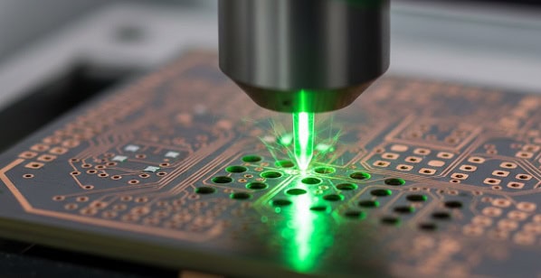
CO₂ & UV Laser Drilling
Dual-wavelength laser systems for optimized drilling: CO₂ laser removes dielectric, UV laser cleans copper pads without thermal damage. Real-time beam monitoring ensures consistent energy delivery across millions of microvia drilling cycles.
Automated Optical Inspection (AOI)
3D AOI systems inspect every panel at multiple stages: post-imaging, post-etch, post-solder mask. Micron-resolution cameras catch trace width variation, microvia presence, and defects invisible to manual inspection — before they propagate to subsequent process steps.
Precision Registration System
CCD camera-based registration achieves ±25µm (±1 mil) layer-to-layer alignment across sequential lamination cycles. Tooling pins, thermal compensation, and real-time measurement ensure stacked microvias align reliably even on large-format panels.
Batch Process Control
Statistical process control (SPC) monitors critical parameters: plating bath chemistry, lamination pressure, imaging exposure dose, etch rate. When any parameter drifts outside control limits, production pauses for correction — preventing defective panels from advancing.
 Laser Drilling — Microvia Formation
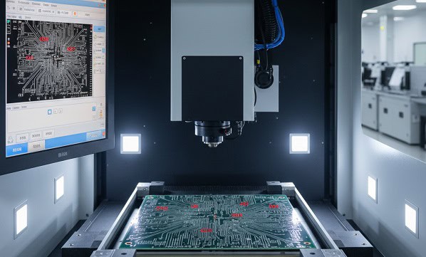 AOI Inspection — Defect Detection
 Sequential Lamination — Build-Up Layers
Registration Accuracy
Layer-to-layer alignment precision
Min Microvia Diameter
Laser drill capability with ±10µm tolerance
First-Pass Yield
HDI production yield rate (1+N+1 structure)
AOI Coverage
Every panel inspected at critical process steps
Want to verify our HDI manufacturing capability before committing to production? We offer virtual facility tours and process documentation.
Request a Facility IntroductionFast Quotation &
Urgent HDI PCB Production
Time-to-market pressure doesn't excuse compromising on quality — but it does demand a manufacturing partner who treats urgency as an engineering problem, not just a premium pricing opportunity. Our rapid quote and express production services are built into our standard workflow, not tacked on as afterthoughts.
2-Hour Engineering Quote Turnaround
Submit your Gerbers, stack-up, and BOM — and receive a detailed quote with DFM feedback within 2 hours during business hours (GMT+8). Our engineering team reviews every HDI design before quoting, so you know the price reflects actual manufacturability, not just an automated calculation that ignores complexity.
📧 Average Response: 90 minutes5–7 Day Urgent Production Available
Standard HDI lead time is 10–12 working days. For urgent projects — prototype validation deadlines, conference demos, investor presentations — we offer express production with 5–7 day turnaround for standard complexity (1+N+1, up to 10 layers). Higher complexity or layer counts scale proportionally, but urgency doesn't compromise process control.
⚡ Rush capability without yield sacrificePriority Queue Access
Urgent jobs bypass standard production scheduling
Real-Time Updates
Daily progress reports during fabrication
Express Shipping
DHL/FedEx international courier included
Same Quality Standards
No shortcuts — full AOI and E-test on all boards
Facing a tight deadline but can't compromise on HDI quality? Let's discuss what's achievable within your timeline.
Request Urgent HDI PCB QuoteChina-Based HDI PCB Manufacturer
with Global Clients
Manufacturing location matters less than manufacturing capability and accountability. We're based in China — factory-direct pricing, no middlemen — but we operate with the engineering transparency, process documentation, and quality consistency that international clients demand. Geography doesn't determine reliability; systems do.
Factory Direct — No Trading Companies
You communicate directly with the engineers who design your process, the technicians who run your panels, and the quality team who inspects your boards. No sales broker three layers removed from production promising capabilities they can't verify. Transparency isn't optional — it's how we operate.
10+ Years Exporting to US, EU, UK
We've been shipping HDI boards internationally since 2013 — which means we understand IPC-6012 Class 3 inspection criteria, UL material requirements, RoHS compliance documentation, and the export paperwork that clears customs without delays. International logistics is a solved problem for us.
English Engineering Support
Our account managers and DFM engineers communicate in English — written and verbal — during your business hours (we accommodate US East Coast, West Coast, and EU time zones). Technical questions get technical answers from engineers, not translation delays through a support queue.
 Our Facility · Direct Access
What Working with a Chinese HDI Manufacturer Should Actually Look Like
The concerns most companies have about overseas PCB manufacturing — communication gaps, hidden substitutions, inconsistent quality — are vendor selection problems, not country problems. When you partner with us, you get direct access to engineering, documented processes, and the accountability that comes from owning the entire production chain.
- Dedicated project manager — one contact for your account, not a rotating support queue
- Video facility tours available for clients who want to see production before committing
- Complete production documentation: DFM report, AOI images, E-test data, export certificates
- IPC-A-600 and IPC-6012 compliance as baseline — Class 2 standard, Class 3 available on request
- Full export package: commercial invoice, packing list, COO, material certs, test records included
Quality Management
Certified processes & systems
UL-Listed Materials
PCB laminates & base materials
Lead-Free Compliance
EU RoHS directive certified
Chemical Compliance
EU chemical safety standards
Want to verify our facility and capabilities before placing your first HDI order? Request a virtual tour and process overview.
Request a Facility IntroductionStable Batch Control
for OEM & EMS Clients
Prototype success means nothing if production batches deliver inconsistent results. For OEMs and EMS partners running repeating orders, batch-to-batch stability isn't a feature — it's the baseline expectation. Our HDI mass production model is built on statistical process control, locked parameters, and the discipline to reject panels that drift outside spec.
Locked Process Parameters
After your pilot run is approved, every process parameter — laser drill energy, lamination pressure, plating current density, imaging exposure dose — is documented and locked. Subsequent batches run on identical settings. No operator discretion, no "similar enough" approximations. Process drift triggers automatic holds and engineering review before panels advance.
Statistical Process Control (SPC)
Critical parameters are monitored using control charts: via diameter distribution, trace width variation, copper thickness uniformity, registration accuracy. When any parameter trends toward control limits — even if still within spec — production pauses for calibration or adjustment. We fix process drift before it produces defects.
Batch Traceability & Documentation
Every production batch is assigned a unique lot number tied to material certs, process logs, inspection results, and final test data. If a field issue surfaces months later, we can trace back to the exact panel, the exact lamination cycle, and the exact process conditions — enabling root cause analysis rather than guesswork.
Batch Yield Rate
Average yield across HDI mass production (12+ months)
Batch-to-Batch Variation
Yield consistency between sequential production runs
Lot Traceability
Full material and process documentation per batch
Field Return Rate
Customer-reported defects (post-assembly failures)
Running repeating HDI production orders and need batch-to-batch consistency you can trust? Let's discuss process control protocols.
Discuss Mass Production RequirementsApplications Suitable
for HDI PCBs
HDI technology isn't appropriate for every design — and forcing HDI complexity onto boards that don't require it wastes both money and lead time. Understanding which applications genuinely benefit from high-density interconnect helps you make the right technology choice for your specific product requirements.
RF & High-Speed Communication
5G modules, WiFi 6E/7, millimeter-wave radar, and RF transceivers demand controlled impedance, minimal via stubs, and tight layer-to-layer registration — requirements standard multilayer fabrication struggles to achieve consistently. HDI enables the signal integrity these designs require.
Industrial Control & Automation
Motion controllers, PLCs, and industrial communication boards increasingly use high-pin-count FPGAs and processors with 0.4–0.5mm BGA pitch. Routing these devices requires microvia fanout capability — making HDI the only practical fabrication approach for compact industrial designs.
Compact Embedded Systems
Wearables, IoT edge devices, portable medical instruments, and handheld measurement tools face strict size constraints while supporting high-speed interfaces (USB, MIPI, PCIe). HDI's routing density advantage is what makes these physically compact designs functionally feasible.
High-Performance Computing
GPUs, AI accelerators, and multi-core server processors generate hundreds of high-speed differential pairs that must maintain signal integrity across dense BGA fanouts. HDI's ability to route between balls and manage controlled impedance through layer transitions is critical for these applications.
When to Choose HDI vs. Standard Multilayer PCB
| Design Characteristic | Standard Multilayer | HDI Required |
|---|---|---|
| BGA Pitch | 0.8mm and larger | 0.5mm and below |
| Routing Density | Low to moderate trace count | High-density signals between components |
| Board Size Constraint | Size not critical | Must minimize PCB area for size/weight |
| Signal Speed | < 1 Gbps typically acceptable | > 5 Gbps requires impedance control |
| Layer Count Goal | Layer count not constrained | Reduce layers via microvias |
| Cost Sensitivity | Lowest $/unit primary goal | Performance/size justifies premium |
Unsure whether your design requires HDI capability or if standard multilayer will suffice? Our engineers can assess your requirements.
Discuss Your HDI Design RequirementsIf Your Design Requires Any of These,
It's Time to Start the Conversation
You don't need finalized Gerbers or a complete BOM to begin. Most HDI projects benefit from early engineering input — stack-up consultation, DFM guidance, material selection — before committing to a design that may be difficult or costly to manufacture.
Scenario One
Microvias & Sequential Build-Up
Your design requires laser-drilled microvias, blind/buried vias, or 1+N+1 (or more complex) sequential lamination structures. You need a manufacturer who treats HDI as core capability, not an occasional specialty service.
Scenario Two
Fine Line & Controlled Impedance
You need 2 mil (50µm) or finer line width/spacing, controlled impedance to ±5% or tighter, and the engineering support to validate your stack-up before fabrication begins — not after yield issues surface.
Scenario Three
Complex Stack-Ups & High Layer Count
Your design pushes 10+ layers with mixed signal/power routing, requires thermal management planning, or involves high-speed differential pairs that demand careful via placement and return path management across layer transitions.
Request Your HDI PCB Quote
& Engineering Review Today
Submit your Gerbers, stack-up requirements, and target specifications — and receive a detailed quote with engineering DFM feedback within 2 hours. No hidden costs. No vague estimates. Just a straightforward answer from engineers who will actually fabricate your boards.
Tell Us About Your PCB Project
Get a customized quote within 24 hours. Our team is ready to help you find the perfect solution for your needs
Email Us
[email protected]
Response within 12 hours
Call / WhatsApp
+86-0755-363091328
Mon - Sat, 9AM-6PM CST
Visit Our Factory
1-4/F Property Office Building, ZhengFeng North Road, Shenzhen, China. 518103
Visit Our Office
(Head Office)1/27, Soi Border 5, Bang Bon Tai,Bang Bon, Bangkok 10150,Thailand