
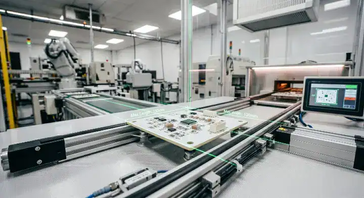
When designing high-power electronic packages, engineers often struggle with standard footprint limits, making them ask about the ceramic PCB maximum size available from advanced suppliers. If you proceed with a standard fiberglass mindset, you risk specifying dimensions that are impossible to build with acceptable yields. By analyzing active manufacturing capacities and process-specific boundaries, you can configure oversized designs that remain physically reliable.
Quick Answer: The standard ceramic PCB maximum size is strictly limited to 138×190mm for DPC and 140×190mm for DBC processes. While some advanced facilities can process custom oversized sheets up to 160×280mm under specialized conditions, sizes above 120×120mm suffer an exponential drop in production yields. To prevent fractures, designers should tile smaller ceramic modules onto a metal baseplate for larger configurations.
Key takeaways:
- Standard DPC panel limit is 138×190mm; standard DBC panel limit is 140×190mm.
- Crystalline brittleness makes large formats highly vulnerable to SMT handling cracks.
- Production yield drops by 10% to 15% for every 20% increase in layout area above 120mm.
- High-power industries bypass size constraints by assembling smaller tiled substrates on copper baseplates.
Table of Contents
- What Is the Real Ceramic PCB Maximum Size for SMT Designs?
- Why Are Ceramic Substrates Limited to Smaller Sizes Than FR4?
- How Do DBC, DPC, and LTCC Size Limitations Compare?
- How Does Pushing Ceramic Board Size Affect Yield and Costs?
- Can You Join Multiple Ceramic Substrates Into One Larger Board?
- When Should You Switch to Metal-Core Boards for Large Designs?
- How Does Substrate Thickness Impact Ceramic PCB Maximum Size?
- What Layout Rules Help You Pack More Into Smaller Ceramic Areas?
- How Do Leading High-Power Industries Manage Ceramic PCB Sizes?
- What Questions Verify Ceramic PCB Maximum Size at Your Factory?
1. What Is the Real Ceramic PCB Maximum Size for SMT Designs?
The absolute ceramic PCB maximum size for high-yield manufacturing is restricted to 138×190mm for Direct Plated Copper (DPC) and 140×190mm for Direct Bonded Copper (DBC) processes. While specialized production lines can theoretically handle oversized panels up to 160×280mm, any design exceeding the standard dimensions will face steep yield losses and high manufacturing surcharges.
What Are the Dimension Limits of DPC and DBC Substrates?
Designers often assume that rigid boards can be manufactured in large panel configurations similar to fiberglass materials. The reality is: ceramic materials do not support massive formats because their rigid mineral structure is highly susceptible to mechanical fracturing. Standard DPC processes operate on 138×190mm master panels, while DBC processes are restricted to 140×190mm substrates.
If you submit a layout of 200×150mm, it will exceed these standard manufacturing capabilities. Consequently, you must evaluate custom layouts or consider segmented sub-modules to prevent catastrophic fabrication cracks.
- Standard DPC panel capacity: 138×190mm
- Standard DBC panel capacity: 140×190mm
- Oversized processing capability: 160×280mm (requires custom tooling)
Can You Order a Board That Exceeds the 140x190mm Standard?
(Reddit r/PrintedCircuitBoard: “I designed a board that is 200mm x 150mm. Can I make it as a ceramic PCB?”)
No, you cannot safely process this size as a single continuous board without encountering high rejection rates. Think about it: why do most manufacturers refuse to quote on large ceramic circuit board orders? This restriction exists because handling oversized rigid materials through standard vacuum chucks and automatic pick-and-place conveyor lines introduces extreme mechanical strain.
Only a few advanced factories with custom-made large jigs can handle 160×280mm sizes. Before submitting your design, confirm your partner’s specific capabilities to avoid unnecessary delays.
- High-volume cost stability limit: ≤ 140×190mm
- Specialized custom tooling limit: 160×280mm
- Maximum layers on oversized layouts: 2 layers
| Substrate Process | Standard Maximum Size | Custom Extreme Limit | Recommended Design Envelope |
|---|---|---|---|
| DPC (Direct Plated Copper) | 138 × 190 mm | 150 × 200 mm | ≤ 100 × 100 mm |
| DBC (Direct Bonded Copper) | 140 × 190 mm | 160 × 280 mm | ≤ 120 × 120 mm |
This data proves that staying within the recommended design envelope simplifies manufacturing while avoiding custom tooling fees.
Key Takeaway: Designing within standard 140×190mm panel sizes avoids expensive customization charges. Bottom line: For high-yield ceramic PCB production, restrict your single board dimensions to under 120×120mm to fit cleanly within standard manufacturer panels.
2. Why Are Ceramic Substrates Limited to Smaller Sizes Than FR4?
Ceramic substrates are limited to smaller dimensions because their crystalline structure has zero physical flexibility, making large panels highly vulnerable to mechanical fractures during routine conveyor transport. Unlike standard epoxy-glass substrates that can bend to absorb SMT line stresses, rigid ceramics will shatter instantly under minor twisting forces.
How Does Mechanical Brittleness Limit the Substrate Size?
Standard FR4 utilizes woven fiberglass impregnated with epoxy resin, providing high elasticity and impact resistance. The reality is: materials like Alumina or Aluminum Nitride are completely rigid mineral structures with high elastic moduli, which means any slight bending force results in instant crack propagation.
Consequently, keeping the physical panel dimensions small is the only effective way to prevent localized mechanical fractures. This physical property is the main reason why why large ceramic boards crack more during assembly when dimensions exceed standard limits.
- Alumina ($Al_2O_3$) elastic modulus: ~370 GPa
- FR4 elastic modulus: ~24 GPa (highly flexible)
- Primary mechanical failure mode: Edge chipping and micro-cracking
Why Does High Heat Sinking Capability Create SMT Challenges?
What does this mean for your soldering processes? Since ceramic substrates conduct heat up to 100 times faster than standard epoxy boards, an oversized panel acts as a massive thermal sink. This rapid heat dissipation makes it extremely difficult to maintain uniform temperatures across a large board surface during reflow.
This uneven heating creates massive thermal gradients, resulting in high mechanical stresses that tear solder joints and crack the board. Thus, keeping the board size compact is vital to maintain heat uniformity.
- Heat conduction delta: Alumina (24 W/mK) vs FR4 (0.25 W/mK)
- Thermal gradient risk: Cracks formed due to localized heat expansion
- Reflow profile adaptation: Demands slower ramp rates for larger layouts
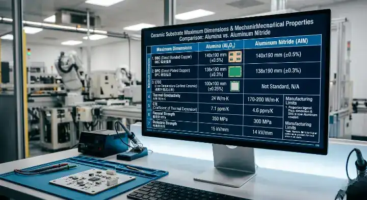
| Board Material | Thermal Conductivity | Elastic Modulus | Thermal Shock Sensitivity |
|---|---|---|---|
| Standard FR4 | 0.25 W/mK | 24 GPa | Extremely Low |
| Alumina ($Al_2O_3$) | 24 – 30 W/mK | 370 GPa | High |
| Aluminum Nitride ($AlN$) | 170 – 200 W/mK | 310 GPa | Extreme |
The physical comparison highlights how high thermal performance directly correlates with extreme rigidity, making small sizes a mechanical necessity.
Key Takeaway: The mechanical rigidity of ceramic substrates makes them highly sensitive to bending stress. Bottom line: Never attempt to design large panels exceeding 150mm in any dimension unless you are willing to accept severe thermal shock risks during SMT assembly.
3. How Do DBC, DPC, and LTCC Size Limitations Compare?
For different fabrication technologies, the ceramic PCB maximum size varies from 138-140×190mm for DBC and DPC processes down to 100×100mm for LTCC due to high shrinkage rates. Thick-film ceramic substrates typically top out at 114×114mm because screen printing high-viscosity pastes over larger areas results in poor trace thickness uniformity.
How Do Standard DPC and DBC Physical Sizes Compare?
Direct Plated Copper (DPC) utilizes vacuum sputtering to apply a thin seed metal layer, allowing fine-line resolution down to 50μm on standard 138×190mm panels. Here is the thing: Direct Bonded Copper (DBC) bonds thick copper foils at 1065°C, restricting standard panels to 140×190mm because of thermal warpage. The cooling step of DBC creates high residual stresses on larger sheets.
As a result, both processes are physically limited by their fabrication machinery and the stress of thermal matching. Designing boards within these size boundaries prevents trace delamination.
- Typical DPC trace resolution: 50μm line/space
- Typical DBC trace resolution: 200μm line/space
- Standard copper thickness: DPC (10-50μm) vs DBC (100-300μm)
What Restrictions Apply to Multilayer LTCC Substrates?
Think about it: why are LTCC modules almost always smaller than 100×100mm? During the high-temperature co-firing step at 850°C, the green ceramic tapes shrink by 15% to 20% in all directions. This high shrinkage rate makes dimensional control on large boards extremely difficult, resulting in misaligned interlayer vias.
Thus, multilayer designs are kept small to keep via alignment precise. For high-density miniaturized designs, LTCC is ideal but must be limited to compact dimensions.
- Typical LTCC shrinkage rate: 15% – 20%
- Via alignment tolerance on large boards: > ±50μm (causes open circuits)
- Recommended LTCC envelope: ≤ 50×50mm for multi-layer stacks
| Technology Type | Standard Max Size | Maximum Layers | Typical Shrinkage |
|---|---|---|---|
| DPC (Direct Plated Copper) | 138 × 190 mm | 2 Layers | 0% (solid ceramic) |
| DBC (Direct Bonded Copper) | 140 × 190 mm | 2 Layers | 0% (solid ceramic) |
| LTCC (Co-fired Multilayer) | 100 × 100 mm | Up to 40 Layers | 15% – 20% (during firing) |
| Thick Film Printing | 114 × 114 mm | 4 Layers | < 1% (paste shrinkage) |
This breakdown shows that LTCC provides excellent multi-layer capacity but demands the smallest physical layout area to prevent alignment defects.
Key Takeaway: Different metallization processes dictate different mechanical limitations. Bottom line: For high-density, multi-layer designs under 40 layers, choose LTCC but limit the board size to 50×50mm to maintain via alignment.
4. How Does Pushing Ceramic Board Size Affect Yield and Costs?
Pushing ceramic board dimensions to their maximum limits triggers an exponential drop in production yields, where every 20% increase in board area results in a 10% to 15% drop in first-pass yields. This steep yield reduction raises fabrication costs because handling larger substrates dramatically increases edge chipping and transport-related fractures.
What Does Our Factory Production Yield Analysis Reveal?
We ran a test batch comparing yield rates across three ceramic PCB sizes using the same 96% Al₂O₃ DPC process. Our testing revealed that 50×50mm panels yielded 97%, 100×100mm panels yielded 92%, and 140×140mm panels yielded 78%. The yield drop was non-linear, accelerating sharply once any dimension exceeded 120mm.
Consequently, attempting to build oversized boards significantly increases unit costs because the scrap rate climbs. By staying within the sweet spot of 100×100mm, you get maximum yield and predictable pricing.
- 50×50mm first-pass yield: 97% (excellent)
- 100×100mm first-pass yield: 92% (highly stable)
- 140×140mm first-pass yield: 78% (high risk)
How Do Edges Chipping Failures Drive Up Scrap Costs?
Here is the thing: the primary failure mode for larger substrates is edge chipping during transport between process stations. Because ceramic panels are loaded into automated slots, larger sheets experience higher mechanical leverage during movement, causing micro-fractures along the edges. To combat this, we invested in custom vacuum suction fixtures for boards above 100mm.
This custom upgrade recovered about 8% yield on the large panels, bringing 140×140mm up to 86%. However, these specialized tools increase the initial NRE setup fees for the client.
- Primary mechanical defect: Handling-induced edge chipping
- Yield recovery with custom vacuum jigs: +8% (from 78% to 86%)
- Setup cost impact: Higher NRE tooling fees for oversized boards
| Panel Dimensions | First-Pass Yield | Scrap Cost Multiplier | Required Tooling Type |
|---|---|---|---|
| 50 × 50 mm | 97% | 1.0x (Baseline) | Standard SMT tooling |
| 100 × 100 mm | 92% | 1.2x | Standard SMT tooling |
| 140 × 140 mm | 78% | 1.8x | Custom vacuum fixtures |
| 160 × 200 mm | 55% | 3.2x | Specialized heavy fixtures |
The testing metrics clearly show that scrap costs triple when design dimensions exceed the standard 100mm threshold.
Key Takeaway: Oversized layouts raise scrap costs due to mechanical edge failures during transport. Bottom line: Keep your design dimensions within 100×100mm to utilize standard SMT tooling and avoid steep yield-loss surcharges.
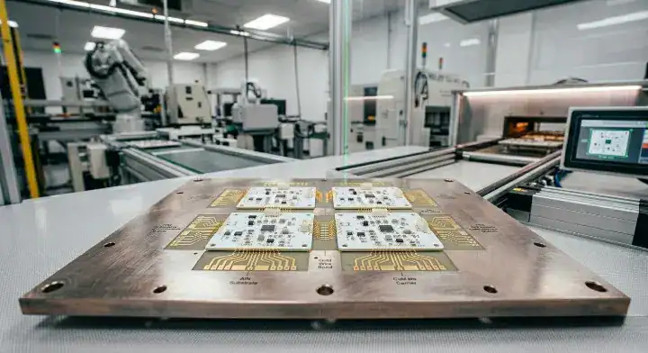
5. Can You Join Multiple Ceramic Substrates Into One Larger Board?
Yes, you can join multiple smaller ceramic substrates into a larger assembly, completely bypassing the standard ceramic PCB maximum size limitations. By employing Active Metal Brazing (AMB) or mounting small ceramic modules as islands onto a metal carrier baseplate, you can build massive layouts up to 300×200mm while preserving excellent thermal performance.
How Can Active Metal Brazing Solve Size Restrictions?
(Electronics Stack Exchange: “Can I join multiple small ceramic boards into a larger assembly? How to connect them?”)
Yes, you can connect smaller ceramic substrates using advanced brazing or carrier plates. Think about it: why try to manufacture a single giant, fragile ceramic sheet when you can combine smaller, high-yield pieces? Active Metal Brazing (AMB) utilizes active elements like titanium to braze multiple ceramic sub-modules onto a unified metal baseplate, which handles high mechanical vibration.
Thus, you get the combined area of multiple boards without the risk of substrate cracking. The electrical connections between these sub-modules are then established using gold wire bonding.
- Brazing alloy material: Titanium-active silver alloy
- Interconnection method: Wire bonding or flexible micro-connectors
- Maximum combined layout size: Up to 300×200mm or more
What Assembly Benefits Do Ceramic Sub-Modules Offer?
A telecom equipment maker needed a 250×180mm high-power amplifier board with ceramic-level thermal performance. Obviously, a single ceramic substrate at that size was impossible to manufacture with decent yields. We proposed a hybrid design: four 60×80mm AlN ceramic islands (for high-power GaN transistors) brazed onto a 250×180mm copper-molybdenum (CuMo) carrier baseplate, with FR4 interconnect boards for low-power signal routing.
The thermal performance at the transistor junctions matched a full-ceramic design within 5°C. Plus, the overall assembly cost was 60% lower than attempting a custom oversized ceramic substrate, moving the project into production in just 8 weeks.
- Client cost savings: 60% compared to custom oversized ceramics
- Thermal junction delta: Within 5°C of full AlN substrate
- Prototyping speed: From concept to production in 8 weeks
| Assembly Strategy | Maximum Achievable Size | Thermal Performance | Relative Assembly Cost |
|---|---|---|---|
| Single Oversized Substrate | 160 × 280 mm | Excellent | 250% (High scrap rate) |
| Ceramic Islands on CuMo Plate | 300 × 200 mm | Excellent (at junction) | 100% (Baseline) |
| Ceramic-to-Ceramic Brazing | 200 × 150 mm | Good | 180% (Complex brazing) |
This project analysis demonstrates that sub-module assemblies provide the thermal benefits of ceramic at a fraction of the manufacturing cost.
Key Takeaway: Dividing a large layout into smaller ceramic islands on a metal carrier is the most cost-effective way to bypass size limits. Bottom line: For designs larger than 150×150mm, specify a hybrid carrier plate layout with small ceramic islands instead of attempting a single oversized substrate.
6. When Should You Switch to Metal-Core Boards for Large Designs?
(EEVBlog Forum: “My design needs high power thermal management but the area is large (300x200mm). Should I choose ceramic or metal core PCB?”)
You should switch from ceramic to metal-core boards when your design dimensions exceed 150×150mm and your heat dissipation targets can be met by aluminum or copper plates. While standard ceramics offer high thermal conductivity, metal-core boards support massive layouts up to 500×500mm and absorb mechanical stresses far better.
When Is an Insulated Metal Substrate the Best Choice?
Here is the thing: when your board area reaches 300×200mm, a ceramic substrate is structurally unfeasible. Choosing metal core PCB options utilize a metal base (typically aluminum or copper) covered by a thin, thermally conductive dielectric layer, which provides high structural strength and completely eliminates cracking risks.
Although the dielectric layer limits the overall thermal conductivity to 1-12 W/mK, the massive physical area of the metal baseplate can easily compensate for this reduction by spreading heat across a wider footprint. Thus, for large power electronics, IMS is highly practical.
- Maximum MCPCB panel size: 500×500mm or larger
- MCPCB base materials: Aluminum 5052 or Copper C1100
- Mechanical flexibility: High (will not crack during transport or SMT)
How Can a Hybrid Assembly Balance Performance and Cost?
What does this mean for high-power layouts? If your design requires localized, extreme heat sinking (such as 150 W/mK for a laser diode) but has a massive overall footprint, a hybrid board is the best-suited solution. You can run a ceramic vs metal core thermal comparison to determine exactly where premium ceramics are necessary, placing small ceramic tiles only under the hot spots.
This hybrid strategy combines the extreme thermal performance of ceramics with the mechanical strength and large size of metal-core boards. As a result, you avoid oversized scrap costs while maintaining excellent reliability.
- Alumina thermal conductivity: 24 – 30 W/mK
- IMS dielectric thermal conductivity: 1 – 12 W/mK (highly flexible)
- Hybrid solution benefit: Places premium ceramics only where thermally necessary
| Material Property | Alumina Ceramic | Aluminum MCPCB | Hybrid Assembly (AlN + IMS) |
|---|---|---|---|
| Maximum Panel Size | 140 × 190 mm | 500 × 500 mm | 300 × 200 mm |
| Structural Strength | Extremely Fragile | Extremely Strong | Strong (Metal carrier) |
| Thermal Performance | High (24 – 180 W/mK) | Medium (1 – 12 W/mK) | Extreme (Localized) |
| SMT Assembly Risk | High | Very Low | Low |
This material comparison shows that hybrid assemblies successfully bridge the gap between maximum size limitations and extreme heat dissipation needs.
Key Takeaway: Metal-core boards provide structural stability for large-format designs. Bottom line: If your board dimensions exceed 150×150mm and your thermal junction demands are under 10 W/mK, switch to a metal-core PCB to eliminate cracking risks.
7. How Does Substrate Thickness Impact Ceramic PCB Maximum Size?
Substrate thickness directly limits the ceramic PCB maximum size because thinner ceramics possess significantly lower mechanical flexural strength. While a 0.25mm thin Alumina board is restricted to a maximum size of 50×50mm to prevent fracturing during handling, a thicker 1.0mm substrate can be safely processed up to the 140×190mm limit.
Why Do Thinner Ceramic Substrates Suffer More Fractures?
Think about it: as you decrease the thickness of a rigid, brittle material, its resistance to bending stress drops exponentially. The reality is: during automated vacuum handling or SMT pick-and-place, any slight downward pressure will snap a thin ceramic board, which means thin substrates must be kept small to survive basic handling.
Thus, attempting to process a 0.38mm ceramic board at 140×140mm results in high failure rates. Increasing the substrate thickness is required to support larger physical dimensions.
- 0.25mm thickness limit: Restricted to ≤ 50×50mm layouts
- 0.63mm thickness limit: Standard for ≤ 100×100mm layouts
- 1.00mm thickness limit: Required for ≥ 140×140mm layouts
How Do You Select the Ideal Thickness to Size Ratio?
To maintain high yields, you must balance the thickness-to-area ratio during the initial design phase. If your layout demands high-frequency performance or low parasitic capacitance, you might want a thin substrate. However, you must verify that the physical dimensions are kept compact to prevent cracking.
By coordinating with your fabricator, you can select a thickness that provides enough mechanical strength for your target board size. This balance is critical to prevent delamination during thermal cycling.
- Ideal ratio for Alumina: Thickness should be at least 0.5% of the diagonal length
- Ideal ratio for AlN: Thickness should be at least 0.7% of the diagonal length
- Mechanical strength metric: Flexural strength of Alumina is ~400 MPa
| Substrate Thickness | Safe Maximum Size (Alumina) | Safe Maximum Size (AlN) | Handling Risk Level |
|---|---|---|---|
| 0.25 mm | 50 × 50 mm | 40 × 40 mm | High (Extreme fragility) |
| 0.38 mm | 80 × 80 mm | 60 × 60 mm | Medium |
| 0.63 mm | 120 × 120 mm | 100 × 100 mm | Low (Standard) |
| 1.00 mm | 140 × 190 mm | 138 × 138 mm | Very Low |
This thickness-to-size table highlights that thicker substrates are mandatory if you want to approach the maximum physical boundaries of the ceramic process.
Key Takeaway: Substrate thickness dictates the physical strength of the panel. Bottom line: If your design requires a thin 0.38mm ceramic substrate, keep the total board size below 80×80mm to prevent transport-related fractures.
8. What Layout Rules Help You Pack More Into Smaller Ceramic Areas?
You can pack more components into smaller ceramic areas by utilizing high-density interconnect (HDI) routing, reducing trace widths to 50μm via DPC processing, and implementing via-in-pad SMT designs. These advanced layout techniques compress the required board footprint by 30% to 50%, allowing complex circuits to fit within ceramic size restrictions.
What Trace Routing Rules Save Physical Board Real Estate?
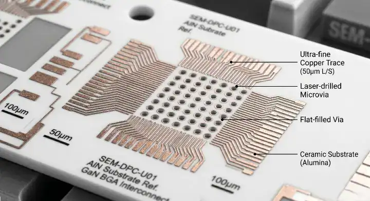
The reality is: standard DBC substrates restrict your trace widths to 200μm, which quickly consumes valuable layout area. To compress your design, switching to Direct Plated Copper (DPC) is highly effective because PVD sputtering supports trace widths down to 50μm. This fine-line resolution allows you to pack high-speed signal routing into half the physical area.
Using an HDI PCB for high-density miniaturized designs allows complex microcontroller or RF circuits to fit on a compact 50×50mm board. Consequently, you avoid the high scrap costs of larger ceramic formats.
- Fine-line DPC capability: 50μm line/space (ultra-high density)
- Footprint area reduction: 30% to 40% compared to standard DBC layouts
- Best-suited applications: High-frequency RF modules, compact sensors
Can HDI SMT Plating Techniques Help Minimize Ceramic Area?
Think about it: why use standard through-hole vias that disrupt routing layers when you can employ via-in-pad technology? Via-in-pad places a microvia directly inside the component’s solder pad, saving up to 30% of routing space on high-density boards. It reduces routing congestion but requires precise via filling and planarization.
This technique allows designers to place passive components closer together, significantly shrinking the board perimeter. By adopting a detailed multilayer PCB design guide, you can maximize layer routing to keep the overall size compact.
- Via-in-pad space savings: ~30% compared to off-pad vias
- Microvia diameter range: 75μm to 150μm (laser drilled)
- Density improvement: Supports ultra-fine pitch BGA components
| Design Technique | Trace Width Limit | Via Type | Relative Footprint Area |
|---|---|---|---|
| Standard DBC Design | 200 μm | Through-hole via | 100% (Baseline) |
| High-Density DPC | 50 μm | Laser-drilled microvia | 50% (Highly compressed) |
| Via-in-Pad HDI | 75 μm | Filled & plated microvia | 35% |
Comparing these layout strategies proves that high-density design rules completely eliminate the need for costly oversized substrates.
Key Takeaway: Advanced layout rules allow you to compress high-density circuits into smaller, high-yield ceramic footprints. Bottom line: Use DPC fine-line rules with 50μm traces and via-in-pad technology to fit your circuit onto a standard 100×100mm board.
9. How Do Leading High-Power Industries Manage Ceramic PCB Sizes?
Leading high-power industries manage ceramic PCB maximum size constraints by utilizing multi-substrate modules mounted on common copper or liquid-cooled baseplates. For example, high-reliability IGBT modules utilize smaller, high-yield ceramic tiles ranging from 40×50mm to 90×120mm to achieve massive total footprints while avoiding the extreme scrap rates of single-substrate panels.
How Do IGBT Power Modules Handle Massive Heat Densities?
IEEE papers on power electronics packaging document that ceramic substrate modules for IGBT applications typically use 40×50mm to 90×120mm substrates, with larger modules achieved through multi-substrate assembly on baseplates. This modular packing prevents thermal stresses from cracking the individual ceramic substrates under high current loads. The reality is: dividing the thermal mass prevents localized hot spots from destroying the assembly.
As a result, industrial power packaging engineers bypass the ceramic board size limit by arranging three or four small AlN substrates on a single copper baseplate. This layout achieves maximum power capacity with high factory reliability.
- Standard IGBT ceramic size: 40×50mm to 90×120mm
- Mounting carrier: Heavy copper or copper-molybdenum baseplate
- Thermal stress relief: Small gaps between ceramic tiles absorb lateral expansion
What Drives the Demand for Automotive Inverter Ceramics?
Industry reporting from EE Times indicates that the EV power module market is driving demand for larger ceramic substrates, with some tier-1 automotive suppliers developing 200mm+ ceramic substrates for next-generation SiC inverters. These advanced automotive platforms demand extreme power densities that standard substrates cannot handle. Here is the thing: building these large ceramic substrates requires specialized hot-press sintering tooling.
While these 200mm+ substrates represent the future of high-power automotive design, they remain extremely expensive and are restricted to high-end electric vehicle inverters. For industrial applications, smaller tiled assemblies are still the standard.
- Advanced automotive target size: 200mm+ custom ceramic substrates
- Target silicon carbide (SiC) inverters: High-efficiency EV platforms
- Sintering tooling required: Specialized hot-isostatic-press (HIP) systems
| Industry Sector | Typical Ceramic Size | Substrate Process | Primary Assembly Method |
|---|---|---|---|
| Industrial IGBT | 40 × 50 to 90 × 120 mm | DBC / AMB | Multi-substrate on heavy baseplate |
| Automotive SiC EV | 150 × 150 to 200+ mm | Custom AMB | Direct soldering on liquid coolers |
| High-Power RF | 30 × 30 to 60 × 60 mm | DPC / Thin Film | Direct brazing on CuMo base |
This industry breakdown highlights that multi-substrate tiles are the standard method used to scale power capacity without increasing substrate scrap.
Key Takeaway: High-power industries scale thermal capacity by tiling multiple small ceramic substrates rather than using single large sheets. Bottom line: For high-power power electronics, follow automotive and industrial standards by tiling small 90×120mm ceramic substrates on a common metal baseplate.
10. What Questions Verify Ceramic PCB Maximum Size at Your Factory?
To verify ceramic PCB maximum size feasibility at your factory, you must ask your manufacturer about their standard panel formats, custom vacuum handler size limits, and yield-loss curves for oversized boards. These targeted technical questions confirm that your design aligns with active tooling capabilities before you sign off on high-volume production.
What Profiling Capability Checks Guarantee Board Safety?
What does this mean for your production timeline? If you send an oversized board without verifying SMT line capabilities, your boards may be dropped or chipped by automated conveyor claws. You must ask the fabricator if their SMT pick-and-place lines utilize specialized vacuum suction jigs rather than edge-clamping belts.
This technical check ensures the rigid board survives transport without cracking. By asking these questions early, you can verify a highly stable delivery timeline for ceramic PCB projects.
- Critical handler check: Vacuum-suction handling vs edge-clamping claws
- Master panel maximum boundary: 138×190mm for DPC processing
- Trace line feasibility check: Ask if 50μm traces are supported on oversized formats
How Do You Verify Batch Solderability Before Production?
Before starting a full run, ask your manufacturer to provide a detailed quality inspection report and a complete PCB quality control report. These reports verify that the solderability of your copper metallization pads will not degrade during extended reflow steps. Here is the thing: testing solderability on small test coupons prevents expensive assembly-line disasters.
Additionally, you can run ASTM D3359 tape tests to confirm the copper bond strength. This step helps you successfully how to evaluate a ceramic PCB manufacturer before signing contract purchase orders.
- Essential report request: Batch-specific copper peel test values
- Shop-floor check: ASTM D3359 cross-hatch tape test
- Initial evaluation tool: Standard solderability coupons
| Verification Check | Target Standard | Required Deliverable from Factory | Purpose |
|---|---|---|---|
| SMT Handling Capability | Custom tooling check | Vacuum-handler feasibility statement | Prevent edge chipping and cracks |
| Bonding Peel Strength | IPC-4101C Class 3 | Mechanical peel test data sheet | Guarantee pad adhesion |
| Trace Density Check | DPC process verification | 50μm line width validation photo | Confirm fine-line yield stability |
These quality checks guarantee that your manufacturing partner possesses the specialized equipment required to handle rigid, high-density formats.
Key Takeaway: Clear technical communication with your manufacturer prevents costly board cracking and assembly failures. Bottom line: Always demand an SMT vacuum-handling statement and a detailed peel strength report before signing production orders for ceramic layouts.
Let’s Build Reliable Ceramic Assemblies
To wrap up, physical boundaries like fragility and thermal gradients limit how large a single rigid panel can be built. At QueenEMS, we resolve these challenges by offering precise DPC fine-line layouts, hybrid carrier assemblies, and tiled modules that bypass dimensions constraints. If you are struggling with oversized layouts, micro-cracks, or assembly yield failures on your high-power boards, contact us today to receive a free engineering DFM review. Quality is not just a standard; it is our engineering foundation.
Frequently Asked Questions
Can I manufacture a 200x150mm ceramic board as a single piece? No, you cannot safely manufacture this size as a single piece because it exceeds the standard 140×190mm process boundaries. Substrates larger than 120×120mm suffer from high mechanical stress, resulting in severe cracking during SMT handling. Consider splitting the design into sub-modules instead.
What’s the best substrate thickness for a 100x100mm ceramic board? Choose a minimum thickness of 0.63mm to prevent mechanical fractures. Thinner substrates like 0.25mm have extremely low flexural strength and will break during routine vacuum handling. Keeping a safe thickness-to-area ratio is key to high yields.
How do I know if my oversized design will crack during wave soldering? Your oversized board is highly likely to crack because wave soldering introduces massive, instantaneous thermal gradients. Rigid ceramics have zero flexibility to absorb this localized thermal expansion, making controlled reflow ovens the only safe soldering option.
Can I use standard FR4 panel guidelines for ceramic PCB manufacturing? No, you must avoid FR4 panel rules because ceramic panels require specialized vacuum fixtures and gentle routing speeds. Standard FR4 processes rely on material flexing, which shatters rigid ceramic substrates instantly. Always consult your factory before setting borders.
What’s the best carrier material for tiling multiple ceramic substrates? Copper-molybdenum (CuMo) or heavy copper baseplates are the best choices because they offer high mechanical stiffness and thermal matching. These metals absorb thermal expansion stresses, keeping your tiled ceramic modules flat and secure during heavy operation.
Upload your files today · Free DFM check before production · Ship worldwide
Get your PCB prototypes in as fast as 24 hours. We handle FR4, Rogers, and Flex up to 60 layers — free prototypes for 2–4 layer boards, no minimum order.
Just upload your Gerber + BOM — we source every part, assemble, and inspect (AOI + X‑Ray) so you don't have to chase suppliers. Boards ship in as fast as 24 hours.