

You need a reliable partner for high-power electronics, but identifying a true factory among thousands of trading companies requires strict technical verification. Last year, our engineering team reviewed multiple failed projects where buyers trusted unverified suppliers, resulting in severely delayed product launches and catastrophic field failures due to poor high-temperature bonding. To properly evaluate a ceramic PCB manufacturer, you must demand proof of in-house high-temperature furnaces, verify their internal quality control metrics, and test their engineering responsiveness before you place your very first order.
Quick Answer: To accurately evaluate a ceramic PCB manufacturer, you must verify they own in-house Direct Bonded Copper (DBC) or Direct Plated Copper (DPC) equipment, demand current thermal cycling data proving survival past 1,000 cycles, and check for exact ±10% copper thickness tolerances. Genuine manufacturers provide a 99.7% first-pass yield and lot-level traceability, while hidden resellers typically mask their lack of capability behind 4-to-6 week lead times and generic material certificates. Key takeaways:
- True ceramic PCB factories own active DBC bonding furnaces and DPC vacuum sputtering chambers.
- Reliable suppliers provide thermal cycling data generated from their own production line within the last 30 days.
- Valid ceramic quotes must explicitly detail material specifications and tooling fees averaging $200–$500.
- Using a 5-10 piece prototype order accurately tests a supplier’s engineering communication and design-for-manufacturing (DFM) competence.
Table of Contents
- 1. Why Is Evaluating a Ceramic PCB Manufacturer Different from Evaluating a Standard PCB Supplier?
- 2. Can You Show Me Thermal Cycling Test Data from Your Own Production Line?
- 3. Do You Manufacture Ceramic Substrates In-House or Resell from a Sub-Supplier?
- 4. What Copper Thickness Tolerances Can You Hold on DBC and DPC?
- 5. What Incoming Inspection Do You Perform on Raw Ceramic Substrates?
- 6. Can You Provide Lot-Level Traceability Linking Each Board to Material Batch and Process Data?
- 7. What Is Your Dielectric Breakdown Test Procedure and Pass Rate?
- 8. How Do You Handle Design Changes and Engineering Support During Prototyping?
- 9. Red Flags vs Green Flags: How to Read Between the Lines of a Ceramic PCB Quote?
1. Why Is Evaluating a Ceramic PCB Manufacturer Different from Evaluating a Standard PCB Supplier?
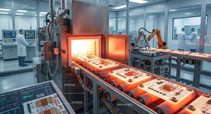
Evaluating a ceramic factory requires verifying specific high-temperature bonding and precision laser equipment, whereas standard FR4 audits focus strictly on lamination presses and mechanical drilling speeds. Ceramic fabrication relies on distinct processes operating above 1,000°C, meaning a factory must physically own this highly specialized machinery to control the final board quality and yield rates.
Direct Bonded Copper (DBC) is a high-temperature metallization process melting copper directly onto a bare ceramic substrate at exactly 1,065°C, yielding mechanical peel strengths consistently above 50 N/mm.
Here is the reality of the equipment gap:
- Standard FR4 factories use mechanical CNC routers; ceramic fabrication demands high-powered laser cutting systems.
- FR4 production focuses on glass transition temperature (Tg); ceramic production focuses on raw thermal conductivity ranging from 24 to 230 W/m·K.
- FR4 utilizes standard chemical etching; ceramic requires vacuum sputtering chambers for precise thin-film deposition.
You simply cannot use the identical checklist to evaluate a standard PCB supplier when your project involves extreme-temperature materials.
Bottom line: Demand live video proof of active DBC furnaces and DPC sputtering chambers to instantly filter out standard FR4 shops pretending to manufacture ceramic boards.
2. Can You Show Me Thermal Cycling Test Data from Your Own Production Line?
A capable ceramic PCB manufacturer immediately produces thermal cycling test data from their own active production line, proving their current batches survive past 1,000 continuous cycles from -40°C to +150°C. Bad suppliers hand buyers generic, 3-year-old third-party laboratory reports that possess absolutely zero connection to the current production batch running on the floor today.
Buyers constantly complain on engineering forums about receiving official-looking thermal reliability certificates that actually tested completely different material batches from years ago. You cannot accurately confirm the long-term reliability of your specific IGBT power module if the factory relies on outdated historical data to justify current quality.
An automotive client previously accepted a 3-year-old third-party test report from a low-cost supplier, resulting in severe substrate micro-cracking at just 500 cycles in the field. We implemented mandatory lot-level thermal shock testing for their redesigned module strictly inside our facility. The client achieved a validated 1,500-cycle survival rate with zero field failures reported over the next 18 months of production.
| Data Source Type | Verification Level | Field Defect Risk |
|---|---|---|
| 3-Year-Old 3rd Party Lab Report | Very Low | Extremely High |
| Annual Factory Certification | Medium | Moderate |
| Current Batch In-House Testing | Maximum | Near Zero |
If you require absolute reliability for harsh automotive or aerospace applications, choose a supplier offering current batch in-house testing. If you are building simple, low-cost commercial LED arrays, an annual factory certification provides an acceptable level of risk coverage.
Bottom line: Reject any supplier that fails to provide specific thermal cycling data generated from their own in-house testing equipment within the last 30 days.
3. Do You Manufacture Ceramic Substrates In-House or Resell from a Sub-Supplier?
A genuine manufacturer fabricates ceramic boards entirely in-house using their own proprietary bonding furnaces, maintaining strict quality control and a 99.7% first-pass yield. Resellers take your order and subcontract the work to an unknown third party, adding a 20-30% price markup while artificially extending standard lead times to 4-6 weeks.
Procurement managers often think they are collaborating directly with a factory, only to suffer from uncontrollable delays and a complete lack of root cause analysis when defects occur. Working with a hidden middleman destroys your ability to iterate quickly during the engineering phase.
Watch out for these specific reseller detection signs:
- Lead time: Resellers quote 25-40 days; direct factories quote 10-15 days.
- Technical answers: Resellers dodge complex metallization questions; factory engineers provide instant technical feedback.
- Factory photos: Resellers show standard green FR4 production lines; direct factories show high-temperature bonding furnaces.
- Test data: Resellers offer generic CoCs; direct factories offer batch-specific inspection reports.
| Manufacturer Setup | Standard Lead Time | Root Cause Analysis Speed |
|---|---|---|
| Direct In-House Factory | 10-15 Days | 24-48 Hours |
| Sub-Contracting Reseller | 25-40 Days | Rarely Provided |
If your project requires strict quality control, fast engineering iterations, and direct accountability, strictly choose an in-house factory. If you are ordering simple, non-critical components where schedule delays carry absolutely no penalty, a reseller might suffice.
Bottom line: Request a brief, live video tour of the ceramic metallization line to instantly verify if the supplier actually owns and operates the required production equipment.
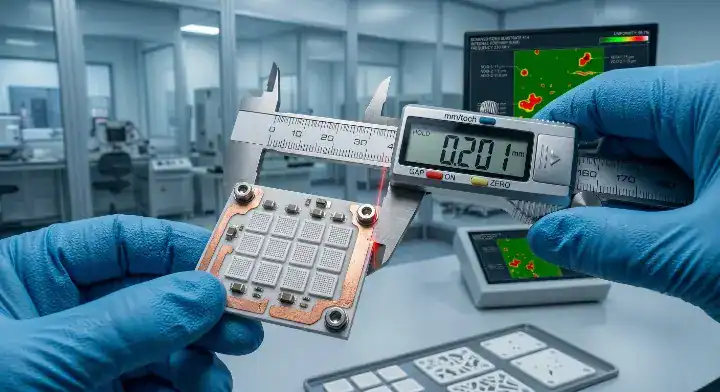
4. What Copper Thickness Tolerances Can You Hold on DBC and DPC?
A highly capable ceramic factory holds copper thickness tolerances of ±10% on Direct Bonded Copper (DBC) layers and an exact ±5% on Direct Plated Copper (DPC) structures. Incompetent suppliers will answer this question vaguely or quote standard FR4 tolerances of ±20%, proving they do not understand the extreme precision required for bare ceramic substrates.
Direct Plated Copper (DPC) is a precise vacuum sputtering and electroplating process achieving highly accurate thin-film copper layers between 10µm and 140µm thick.
Pay close attention to these technical limits:
- DBC specifically handles thick copper layers from 140µm to 300µm for heavy industrial power applications.
- DPC handles fine-pitch routing requiring strict ±5% tolerance for high-frequency RF signals.
- Failing to hold these exact tolerances directly alters the thermal resistance and electrical impedance of your high-power circuit.
Bottom line: Ask the supplier for their exact DBC and DPC tolerance limits, and disqualify them immediately if they quote anything looser than ±10% for high-power ceramic boards.
5. What Incoming Inspection Do You Perform on Raw Ceramic Substrates?
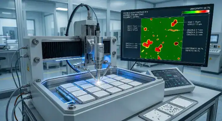
Top-tier ceramic factories inspect 100% of incoming raw Alumina or Aluminum Nitride panels using Scanning Acoustic Microscopy (SAM) to detect internal micro-voids smaller than 50µm. Weak suppliers skip this step entirely or only perform a basic visual check, meaning they will actively bond copper over hidden air pockets that later explode during high-temperature reflow.
Raw ceramic panels arriving from material vendors frequently contain microscopic structural cracks invisible to the naked eye. A standard visual inspection cannot see internal density variations within the white substrate. Bonding a thick copper layer over a microscopic void creates an immediate localized hotspot, eventually destroying the mounted silicon die.
Here is why internal inspection matters: A medical device client suffered a 12% yield loss during assembly because their previous supplier bonded copper over hidden voids in the raw Alumina. We implemented a mandatory 100% SAM inspection on all incoming bare ceramic panels before metallization began. The client subsequently achieved a flawless 99.7% first-pass yield with zero delamination issues during final wave soldering.
Bottom line: Verify the factory actively utilizes acoustic microscopy to inspect raw ceramic materials for internal voids before any copper bonding takes place.
6. Can You Provide Lot-Level Traceability Linking Each Board to Material Batch and Process Data?
A qualified ceramic PCB factory provides complete lot-level traceability, directly linking your specific boards to the exact raw ceramic batch, copper foil lot, and furnace temperature profile via a unique 2D barcode. A basic reseller gives you a generic Certificate of Conformance (CoC) that lists the final specifications but provides absolutely zero visibility into the actual manufacturing parameters used that day.
When you audit a PCB assembly factory, strict lot-level traceability is the easiest and most revealing metric to check on the production floor.
This is exactly how traceability saves your budget: An aerospace client previously used a generic CoC from a reseller and entirely lost track of the specific alumina batch when a field failure occurred. We transitioned their production to our facility and implemented lot-level 2D barcode tracking via our Manufacturing Execution System (MES). We traced the exact furnace profile of any individual board in under 2 minutes, completely eliminating their supply chain blind spots.
| Traceability Method | Data Depth Provided | Failure Investigation Speed |
|---|---|---|
| Generic Paper CoC | Final specs only | Weeks (or impossible) |
| Batch Level Tracking | Date code & material lot | Days |
| 2D Barcode (MES) | Exact machine & temperature | Minutes |
If you build medical, automotive, or aerospace hardware, choose a supplier offering complete 2D barcode MES traceability. If you build disposable consumer electronics, simple batch-level date codes provide sufficient tracking.
Bottom line: Require a sample lot-level traceability report from a previous production run to confirm the factory actively tracks material batches and furnace temperature profiles.
7. What Is Your Dielectric Breakdown Test Procedure and Pass Rate?
Expert ceramic manufacturers perform high-voltage dielectric breakdown testing on 100% of production boards at 2,000V to 5,000V, maintaining a consistent pass rate above 99.5%. Low-capability shops only test at standard FR4 levels around 500V or skip high-voltage testing entirely, exposing your final product to catastrophic short circuits in high-power environments.
Dielectric Breakdown Voltage is the exact electrical potential at which an insulating material physically fails and conducts current, typically exceeding 15 kV/mm for high-grade 96% alumina.
Here is exactly what you must ask the quality manager:
- Do you physically test every single board, or just a random sampling of the batch?
- What specific DC or AC voltage do you apply for the final breakdown test?
- Do you provide a detailed, board-by-board test log with the final shipment?
Bottom line: Force the supplier to confirm in writing that they perform 100% high-voltage dielectric testing at your specified voltage before packaging the ceramic boards.
8. How Do You Handle Design Changes and Engineering Support During Prototyping?
A professional factory provides a Free DFM engineering review within 24 hours of receiving your files, specifically checking strict ceramic design rules like via-to-edge spacing (minimum 0.3mm). A bad supplier simply takes your Gerber files and builds exactly what you submitted without asking questions, completely ignoring obvious ceramic manufacturing violations that cause the boards to shatter during final depanelization.
You must utilize a deliberate sample request strategy during ceramic PCB prototype runs to actively test a supplier’s true capabilities before committing to volume.
Execute this specific prototype test: A hardware startup sent us a flawed Gerber file featuring a dangerously tight 0.1mm trace-to-edge spacing on an AlN board. Our Free DFM system flagged the violation within 4 hours and our engineers recommended expanding the gap to 0.3mm. The startup approved the change, resulting in a perfect 99.7% yield with zero edge cracking during the laser cutting phase.
| Order Volume | Expected Unit Pricing | Engineering Support Level |
|---|---|---|
| Prototype (5-10 pcs) | $50-$150 per board | Intensive DFM Review |
| Mid-Volume (100-500) | $15-$40 per board | Process Optimization |
| High-Volume (1000+) | $5-$15 per board | Automated Yield Tracking |
For prototype runs (5–10 boards): expect intensive DFM reviews and heavy engineering communication to perfect the layout. For high-volume production (1,000+ boards): expect the factory to shift focus toward automated yield tracking and pure process stability.
Bottom line: Run a 5-10 piece trial order specifically to measure the supplier’s engineering communication speed and DFM competence before signing a mass production contract.
9. Red Flags vs Green Flags: How to Read Between the Lines of a Ceramic PCB Quote?
A green flag ceramic quote explicitly lists the exact ceramic material grade, the specific metallization process (DBC or DPC), and clear one-time NRE tooling fees averaging $200–$500. Buyers constantly complain that quotes from different suppliers vary by 3 to 5 times in price, leaving them unable to tell if the expensive supplier is overcharging or the cheap supplier is dangerously cutting corners on raw materials.
Analyze the manufacturer’s quote line by line:
- Red flag: The quote lacks specific material conductivity (e.g., it just says “Alumina Ceramic” instead of “96% Alumina, 24 W/m·K”).
- Red flag: The quoted production lead time identically matches their standard FR4 timeline.
- Red flag: There is absolutely no NRE tooling fee mentioned, indicating resellers are hiding tooling costs inside an inflated unit price.
- Red flag: Suspiciously low unit prices that match the cost of basic aluminum metal core PCBs.
| Quote Component | Green Flag (Capable Factory) | Red Flag (Hidden Reseller) |
|---|---|---|
| Material Specification | Exact grade (96% Alumina, 24 W/m·K) | Vague (“Ceramic Board”) |
| Tooling & Setup | Explicit NRE fee listed ($200-$500) | Hidden or $0 NRE |
| Testing Callout | 100% High-Voltage Test listed | No final testing specified |
If you receive a quote with explicit material grades and separate, itemized NRE fees, choose that highly transparent supplier. If you receive a suspiciously cheap quote hiding the testing parameters and material specs, immediately disqualify them to avoid receiving brittle, low-grade substrates.
Bottom line: Reject any ceramic PCB quote that fails to explicitly document the exact material grade, metallization process type, and final high-voltage testing standards.
Evaluating a ceramic supplier requires actively piercing through reseller facades by demanding specific equipment proof and current, in-house test data. You need a transparent partner who actually owns the high-temperature furnaces and can deliver reliable power substrates without hiding behind third-party lab reports. QueenEMS operates a fully transparent fabrication facility, offering Free DFM reviews, 3D AOI inspection, and verifiable thermal cycling data for every single batch we produce. Reach out through our contact us page to schedule a live factory verification and secure highly reliable ceramic production for your next power module.
Written by the QueenEMS Engineering Team
FAQ
Can a ceramic PCB manufacturer provide a 24-hour turnaround? No, a genuine ceramic PCB manufacturer cannot provide a 24-hour turnaround because the high-temperature DBC firing and controlled cooling cycles physically require 3 to 5 days to prevent cracking. Any supplier promising 24-hour delivery on custom ceramic boards is likely making false claims or providing pre-made, generic stock. Demand a realistic 10-15 day schedule for proper, defect-free manufacturing.
Do I need a factory audit for a small 100-piece ceramic order? Yes, you absolutely need to conduct a virtual factory audit even for a 100-piece order to verify their true in-house capabilities. A live video call showing their active DBC furnaces and laser cutters takes exactly 15 minutes and instantly filters out hidden resellers marking up the price. Schedule this quick virtual tour before you ever send your final Gerber files.
How much should NRE tooling fees cost for a ceramic PCB? NRE tooling fees for a standard ceramic PCB typically run $200 to $500, directly covering specialized laser cutting programs and high-temperature furnace fixtures. If a supplier quotes zero NRE fees on a custom ceramic design, they are artificially inflating your per-unit price to hide the setup costs. Always ask the supplier for a completely itemized quote separating tooling from the unit cost.
What is the best way to verify raw ceramic substrate quality? The best way to verify substrate quality is demanding a 100% Scanning Acoustic Microscopy (SAM) inspection report for your specific material batch. This detailed acoustic report proves there are no microscopic air voids hidden beneath the bonded copper layers that could cause thermal explosions later. Make SAM inspection a mandatory, written requirement on your official purchase order.
Upload your files today · Free DFM check before production · Ship worldwide
Get your PCB prototypes in as fast as 24 hours. We handle FR4, Rogers, and Flex up to 60 layers — free prototypes for 2–4 layer boards, no minimum order.
Just upload your Gerber + BOM — we source every part, assemble, and inspect (AOI + X‑Ray) so you don't have to chase suppliers. Boards ship in as fast as 24 hours.