
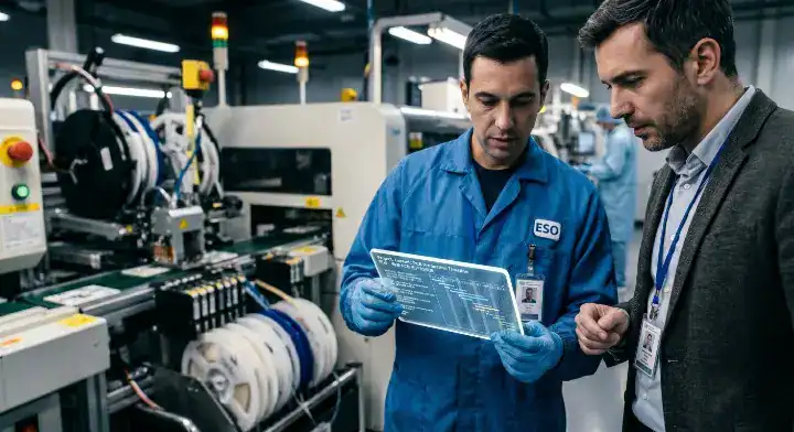
Quick Answer: Ceramic board production requires 3 to 6 weeks standard delivery because high-temperature sintering and custom metallization take significantly longer than standard FR-4 processing. You can slash this turnaround to 10-15 days for prototypes by utilizing DPC manufacturing with standard 1oz copper on 96% alumina substrates. Key takeaways:
- Standard DBC processing takes 3-4 weeks minimum.
- Specifying non-standard copper adds 5-7 days.
- Rounded laser routing severely delays production.
- Rush orders cost 30-50% more but lower yields by 5-10%.
Table of Contents
- How Long Is Ceramic PCB Lead Time for Different Processes?
- Why Ceramic Board Production Takes 3-6 Weeks vs FR4
- Which Ceramic Substrate Manufacturing Method Is the Fastest?
- What Design Choices Add Weeks to Your Ceramic PCB Lead Time?
- How Copper Thickness Affects Ceramic Board Turnaround Time
- Can You Get a Ceramic PCB Prototype in Under 2 Weeks?
- What File Formats Speed Up Ceramic Substrate Processing?
- How Material and Substrate Availability Impact Delivery
- What Are the True Costs of Rushing a Ceramic PCB Lead Time?
- How to Plan Your Ceramic Board Project for On-Time Delivery
High-power projects frequently stall because rigid material fabrication takes drastically longer than standard fiberglass. You might secure FR-4 boards in days, but waiting a month for alumina components completely disrupts your rapid development cycle. We can fix this by adjusting your substrate choices and panel routing methods before sending data to the factory. Our guide reveals why ceramic PCB lead time exceeds normal schedules and how you can accelerate your delivery by 40% using smart PCB fabrication lead time factors.
How Long Is Ceramic PCB Lead Time for Different Processes?
The ceramic PCB lead time varies entirely by process, ranging from 2 weeks for thin-film circuits up to 6 weeks for LTCC boards. Factories schedule these timelines based on the specific metallization chemistry and thermal curing hours required.
Average Delivery Timelines
Different manufacturing methods dictate your absolute minimum waiting period. Thick film and Direct Plated Copper (DPC) generally ship faster than high-heat bonded alternatives.
- DBC boards require 3-4 weeks.
- DPC boards require 2-3 weeks.
- LTCC boards require 4-6 weeks.
- Thick/Thin film boards require 2-3 weeks.
Impact of Industry Standards
Adhering to strict aerospace or military guidelines adds significant inspection hours to your project. IPC-6012DS specifies qualification and performance requirements for rigid printed boards used in space applications, dictating tight dimensional tolerances that extend processing times. Here is the truth: skipping these mandatory validation steps to save time will result in catastrophic field failures. Key Takeaway: Bottom line: Plan for a baseline of 4 weeks when ordering standard Direct Bonded Copper boards for high-reliability applications.
| Process Type | Standard Turnaround | Best Application |
|---|---|---|
| DPC | 2-3 Weeks | LEDs and Prototypes |
| DBC | 3-4 Weeks | Power Modules |
| LTCC | 4-6 Weeks | RF/Microwave |
| Analysis: Vacuum-based DPC methods consistently outperform furnace-based DBC methods in sheer manufacturing speed. |
Why Ceramic Board Production Takes 3-6 Weeks vs FR4
Ceramic board production takes 3-6 weeks because factories do not stock pre-bonded copper-clad laminates, whereas standard FR-4 ships in 3 days due to mass-produced raw materials. You must wait for individual substrate sizing and custom metal bonding for every single batch, resulting in heavily restricted daily output.
The Material Stocking Problem
Users on the Reddit r/PrintedCircuitBoard forum frequently ask why ceramic quotes hit 4 weeks while standard fiberglass arrives by the weekend. Factories keep thousands of FR-4 panels ready for immediate etching, but brittle alumina requires custom fabrication from the ground up.
- No universal pre-clad stock exists for ceramics.
- Each batch requires its own custom metallization phase.
- Rigid boards lack continuous assembly line speed.
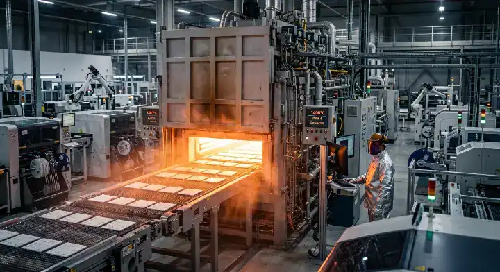
High-Temperature Bonding Limits
DBC (Direct Bonded Copper) is a metallization process utilizing high-temperature oxidation to fuse heavy copper. It requires bonding at 1065°C, demanding several hours for a single furnace cycle. Small batch customization heavily restricts factory throughput compared to continuous FR-4 lines. But it gets worse: rushing a cooling cycle instantly cracks the substrate. Key Takeaway: Bottom line: Accept that brittle materials require custom sequential processing rather than fast parallel manufacturing.
| Substrate Material | Raw Material State | Factory Processing Style |
|---|---|---|
| Standard FR-4 | Pre-laminated sheets | Continuous mass line |
| Alumina / AlN | Bare white ceramic | Small batch custom bonding |
| Analysis: The absence of ready-to-etch pre-laminated sheets adds a mandatory 1-2 week metallization phase to all rigid orders. |
Which Ceramic Substrate Manufacturing Method Is the Fastest?
Direct Plated Copper (DPC) is the fastest ceramic manufacturing method, delivering in 2-3 weeks because it utilizes semiconductor-style vacuum sputtering instead of high-temperature bonding. This modern approach eliminates the need for prolonged furnace baking, which means your boards move into the photoetching phase much faster.
DPC Vacuum Sputtering Speed
DPC creates an extremely thin, precise titanium/copper seed layer in a matter of hours. This process bypasses the extreme thermal requirements of older techniques.
- Vacuum sputtering replaces slow furnace baking.
- DPC achieves high precision on the first pass.
- Plating times remain highly predictable.
Why DBC Takes Considerably Longer
Furnace-based bonding naturally restricts how many panels a ceramic PCB manufacturer can process in a single shift. Engineers must carefully monitor heating and cooling gradients to prevent substrate fracturing. Here is the truth: forcing a DBC furnace to cool faster than 2°C per second destroys the entire batch. Key Takeaway: Bottom line: Specify the DPC process on your manufacturing drawings if delivery speed is your absolute highest priority.
| Manufacturing Method | Bonding Mechanism | Processing Speed |
|---|---|---|
| Direct Plated Copper (DPC) | Vacuum Sputtering | Fast (Hours) |
| Direct Bonded Copper (DBC) | High-Temp Oxidation | Slow (Days) |
| Analysis: Vacuum sputtering technologies offer a 30% reduction in raw manufacturing time compared to traditional thermal oxidation. |
What Design Choices Add Weeks to Your Ceramic PCB Lead Time?
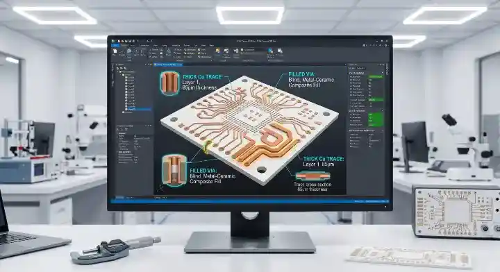
Requesting non-standard copper thickness above 2oz, specifying filled vias, and demanding full laser routing add 5 to 7 days to your ceramic PCB lead time. Every specialized feature you include forces the factory to pull your boards off the standard automated line for manual engineering intervention.
Routing and Via Filling Delays
Using a laser to cut fully rounded board outlines takes drastically longer than scoring straight lines. Additionally, via filling requires multiple plating passes and planarization.
- Laser scribing straight edges takes minutes per panel.
- Full laser routing takes hours per panel.
- Filled vias add 2-3 days for extra chemical plating.
Analyzing Real Factory Data
We tracked our production data over 6 months and found that non-standard copper (>2oz), filled vias, and rounded outlines consistently added 5-7 days to lead times. We shared this data with a repeat automotive client, who adjusted their next design to use 1oz copper with PTH vias and straight edges. But it gets worse for unoptimized designs: their previous lead time was 25 days, and our changes dropped it to 16 days — a 36% reduction. Key Takeaway: Bottom line: Use standard plated-through holes and straight laser-scribed edges to strip a full week from your production schedule.
| Design Feature | Standard Alternative | Time Penalty |
|---|---|---|
| Filled Vias | Plated-Through Holes (PTH) | + 2-3 Days |
| Full Rounded Routing | Straight Laser Scribe | + 1-2 Days |
| > 2oz Heavy Copper | Standard 1oz / 2oz | + 2-3 Days |
| Analysis: Compounding multiple non-standard design features exponentially increases the likelihood of factory delays and yield drops. |
How Copper Thickness Affects Ceramic Board Turnaround Time
Custom copper thicknesses beyond the standard 1oz or 2oz require specialized plating cycles, adding 3-5 days to standard production schedules. Factories must carefully control the chemical deposition rate, because rapid plating creates uneven surfaces that compromise subsequent assembly stages.
Standard vs Custom Plating
Most fabrication facilities stock standard chemical baths calibrated for 35μm or 70μm thickness. Demanding heavy copper forces technicians to run multiple custom cycles.
- 1oz (35μm) copper runs on rapid automated lines.
- Heavy copper demands slow, monitored deposition.
- Uneven plating leads to severe assembly defects.
DBC Heavy Copper Considerations
Heavy copper on rigid substrates creates extreme thermal stress. We frequently resolve assembly cracking issues with ceramic boards by balancing the copper layers accurately. Here is the truth: unmatched copper weights on the top and bottom layers will cause the panel to warp and shatter during the plating process. Key Takeaway: Bottom line: Stick to symmetric 1oz or 2oz copper weights to maintain rapid, predictable factory turnaround times.
| Copper Weight | Processing Speed | Defect Risk |
|---|---|---|
| 1oz (35μm) | Fastest | Lowest |
| 2oz (70μm) | Fast | Low |
| 3oz+ Heavy Copper | Slowest | High |
| Analysis: Exceeding 2oz copper severely disrupts standard factory flow, requiring dedicated engineering oversight and prolonged chemical baths. |
Can You Get a Ceramic PCB Prototype in Under 2 Weeks?
Yes, you can get a ceramic PCB prototype in 10-15 days by selecting a DPC process with standard 1oz copper on a 96% Al₂O₃ substrate. Users on the Electronics Stack Exchange often doubt rapid turnarounds are possible, but simplifying the layer count and material choice guarantees a fast delivery.
Simplifying the Prototype Build
Your prototype does not always need the absolute highest thermal conductivity during initial functional testing. Choosing readily available materials eliminates procurement waiting periods completely.
- Select 96% Al₂O₃ instead of rare AlN.
- Keep the design to a single or double layer.
- Submit a perfectly clean, error-free data package.
An EV Startup Success Story
An EV startup needed 20 pieces of AlN prototype boards for a battery management system, but their initial quote from another supplier was 5 weeks. We proposed switching from AlN to 96% Al₂O₃ for the prototype phase and using DPC instead of DBC. By making these changes, we delivered 20 boards through our rapid PCB prototyping service in 12 working days at a 40% lower cost, saving them 3 weeks on their timeline. Key Takeaway: Bottom line: Downgrade your prototype material to standard 96% alumina to bypass weeks of supply chain waiting.
| Material Choice | Application | Typical Prototype Time |
|---|---|---|
| 96% Al₂O₃ | Initial Validation | 10 – 15 Days |
| Aluminum Nitride (AlN) | Final Production | 21 – 35 Days |
| Analysis: Utilizing standard materials for functional testing drastically accelerates the product development life cycle. |
What File Formats Speed Up Ceramic Substrate Processing?
Submitting full RS-274X Gerber files accelerates engineering reviews, shaving 2 to 3 days off your ceramic PCB lead time compared to submitting DXF or PDF files. Clean Gerber data allows factory CAM software to automatically generate production tooling without manual human translation.
The Superiority of Gerber Files
Gerber files provide explicit machine coordinates for every single copper pad and drill hole. This mathematical precision eliminates the ambiguity that plagues mechanical drawing formats.
- RS-274X natively defines all board parameters.
- DXF files often lose scale and layer data.
- PDF formats require complete manual redrawing.
Avoiding PDF Translation Delays
When you submit a mechanical PDF, a factory engineer must manually redraw your entire circuit into their proprietary software. But it gets worse: manual redrawing introduces human error, requiring multiple back-and-forth email approvals that stall production for days. Key Takeaway: Bottom line: Export your designs strictly in RS-274X or ODB++ formats to guarantee immediate factory processing.
| Submission Format | Factory Processing Time | Error Risk |
|---|---|---|
| RS-274X Gerber | 1-2 Hours | Very Low |
| ODB++ | 1-2 Hours | Very Low |
| DXF / PDF | 2-4 Days | Very High |
| Analysis: Native electronic manufacturing formats entirely eliminate the need for manual human translation and subsequent approval delays. |
How Material and Substrate Availability Impact Delivery
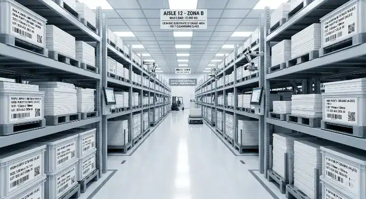
Using standard 96% Al₂O₃ at 0.635mm thickness ensures zero material wait time, while ordering rare 99.6% Al₂O₃ or specialized AlN adds 2-3 weeks just for material procurement. Supply chain shortages heavily dictate your delivery schedule before manufacturing even begins.
Standard Alumina vs Custom AlN
Most factories keep 96% alumina in standard sizes readily available on their shelves. You should read our guide on maximum size constraints for ceramic substrates to understand how panel sizing works.
- 0.635mm Al₂O₃ is highly stocked globally.
- 99.6% purity requires special order minimums.
- AlN procurement takes 2-4 weeks minimum.
Supply Chain Market Pressures
Industry analysis from Electronic Design shows ceramic substrate demand grew 15-20% annually from 2023-2025, driven by EV power modules and 5G infrastructure. Here is the truth: this massive market demand puts intense pressure on already constrained supply chains, making rare materials exceptionally hard to source quickly. Key Takeaway: Bottom line: Base your designs around 0.635mm 96% Al₂O₃ to shield your project from global supply chain shortages.
| Substrate Material | Factory Stock Level | Procurement Delay |
|---|---|---|
| 96% Al₂O₃ (0.635mm) | High | None |
| 99.6% Al₂O₃ | Low | 1 – 2 Weeks |
| Aluminum Nitride (AlN) | Very Low | 2 – 4 Weeks |
| Analysis: Designing around commonly stocked factory materials entirely neutralizes unpredictable global procurement delays. |
What Are the True Costs of Rushing a Ceramic PCB Lead Time?
Rushing your ceramic PCB lead time typically incurs a 30-50% surcharge but only compresses the delivery schedule by 30-40%, often causing a 5-10% drop in yield. Factories achieve faster turnaround times by overriding standard cooling queues, which directly compromises the material’s structural integrity.
Financial and Yield Trade-Offs
Users on the EEVBlog Forum frequently ask if paying a massive premium for a 15-day DBC turnaround is worth the cost. Rushing the process forces the factory to skip beneficial longer soaking times.
- Surcharges run from 30% to 50% extra.
- Rushed cooling increases micro-fracture risks.
- Yield rates drop because of thermal stress.
Smart Alternatives to Rushing
Instead of paying a premium to break factory speed limits, you can achieve similar timelines by utilizing a quick turn PCB assembly partner and optimizing your CAD data. But it gets worse: if a rushed batch fails quality control due to thermal cracking, you will end up waiting another 4 weeks for a reprint anyway. Key Takeaway: Bottom line: Optimize your Gerber design for speed rather than paying a 50% financial penalty for rushed factory processing.
| Production Speed | Cost Surcharge | Yield Impact |
|---|---|---|
| Standard (4 Weeks) | Base Price | Optimal Yield |
| Expedited (2.5 Weeks) | + 30% – 50% | 5% – 10% Yield Drop |
| Analysis: Expedited manufacturing inherently sacrifices thermal soaking stability, resulting in higher defect rates and inflated unit costs. |
How to Plan Your Ceramic Board Project for On-Time Delivery
Planning your production requires adding a 2-week buffer for material sourcing and finalizing all Gerber data 4 weeks before your target assembly date. Building a realistic procurement timeline prevents last-minute panic and expensive expedited shipping fees.
Creating a Sourcing Timeline
A successful project launch requires working backward from your product release date. You must account for engineering questions, material delays, and unexpected quality control holds.
- Finalize CAD data 6 weeks prior to assembly.
- Confirm material stock 5 weeks prior.
- Approve all factory tooling immediately.
Finalizing Engineering Data
Learning how to order a PCB prototype correctly involves responding to factory engineering queries within 24 hours. Here is the truth: a factory will completely halt your order and reset your lead time if you ignore a tooling question for three days. Key Takeaway: Bottom line: Submit your finalized Gerber data 6 weeks before your required delivery date to guarantee stress-free procurement.
| Planning Phase | Action Required | Timeline Marker |
|---|---|---|
| Design Lock | Submit Gerber Files | Week 1 |
| Factory EQ | Answer Engineering Questions | Week 1 – 2 |
| Fabrication | Monitor Production Status | Week 3 – 6 |
| Analysis: Proactive communication during the initial engineering question phase prevents week-long delays from halting the factory floor. |
We know that waiting a month for critical power modules paralyzes your engineering timeline. By switching to standard 96% alumina, selecting the DPC process for prototypes, and using straight laser-scribed edges, you can successfully bypass the worst supply chain bottlenecks. Your material choices directly dictate your speed to market.
You do not have to navigate these complex procurement timelines alone. QueenEMS provides transparent scheduling, fast-track DPC prototyping, and reliable mass production for your most demanding projects. Reach out and contact us today to analyze your Gerber files for speed optimization. We stand by our promise to deliver high-reliability substrates exactly when you need them.
FAQ
Can I get a DBC ceramic board manufactured in 5 days? No. You must allocate at least 3 weeks for standard DBC processing. The high-temperature oxidation bonding requires slow, controlled furnace cycles that physically cannot be compressed into a 5-day window without shattering the ceramic core. Switch to DPC if you require faster prototype delivery.
What is the fastest way to get an AlN substrate prototype? Use standard 1oz copper and simple plated-through holes. Avoiding complex features like filled vias or heavy copper layers strips 5 to 7 days off your production timeline. Always submit clean RS-274X Gerber files to prevent manual engineering delays.
How do I know if my design is slowing down production? Yes, you can spot slow designs by checking your board outlines and via structures. If your design utilizes fully rounded routing instead of straight laser score lines, or mandates custom copper thicknesses above 2oz, you are adding weeks to your lead time. Simplify these parameters to accelerate delivery.
Does using standard FR-4 rules apply to ceramic lead times? No. You must plan for a completely different supply chain cycle because factories do not stock pre-laminated ceramic panels. While FR-4 takes days, rigid materials require custom metallization for every order, pushing timelines to 3-6 weeks.
Is paying the 50% rush fee worth the cost? No. You will severely increase your defect risk because expedited processing often forces the factory to accelerate thermal cooling cycles. This rapid cooling introduces microscopic stress fractures that reduce your overall yield by up to 10%. Optimize your design for speed instead.
Upload your files today · Free DFM check before production · Ship worldwide
Get your PCB prototypes in as fast as 24 hours. We handle FR4, Rogers, and Flex up to 60 layers — free prototypes for 2–4 layer boards, no minimum order.
Just upload your Gerber + BOM — we source every part, assemble, and inspect (AOI + X‑Ray) so you don't have to chase suppliers. Boards ship in as fast as 24 hours.