
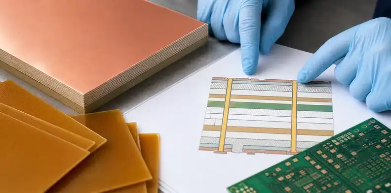
Quick Answer: A core and a prepreg from the same laminate family are not automatically interchangeable electrical layers. Their glass style, resin content, pressed thickness, and final copper environment can differ, which changes impedance, delay, and fabrication behavior. Approve the finished stack-up by layer and pressed condition, not by a single family name copied into a purchase order.
| Question | Core | Prepreg |
|---|---|---|
| What arrives at the fabricator? | Cured laminate, usually copper-clad | Resin-impregnated reinforcement for lamination |
| What happens in the press? | Acts as a defined laminate layer | Resin flows and cures, bonding adjacent layers |
| Which thickness matters to the model? | Specified finished core construction | Expected finished pressed dielectric thickness |
| Can one Dk value describe both? | Not automatically; check the construction and applicable supplier data for each controlled layer | |
- Core is already cured laminate with copper; prepreg is resin-coated reinforcement that changes during lamination.
- The same product family can have different electrical behavior in different constructions.
- Press-out and copper distribution determine the finished dielectric thickness used by impedance calculations.
- A stack-up sign-off should identify the exact construction for each controlled layer.
Core versus prepreg becomes a costly misunderstanding when a high-speed design is quoted as though every dielectric from one material family has the same properties. It does not. A core arrives as a defined cured laminate. A prepreg becomes part of the board only after heat, pressure, copper pattern, and resin flow turn it into a pressed dielectric. Both may carry the same material-family label, but they do not necessarily produce the same effective electrical layer.
The PCB material library helps select a laminate family. This article covers the construction question that follows: what must be controlled when the selected material becomes a real multilayer stack-up.
Table of Contents
- What changes between a core and a prepreg
- Why resin content changes electrical behavior
- How press-out changes impedance geometry
- Which stack-up layers need exact construction callouts
- How copper distribution affects lamination assumptions
- How to approve an equivalent material without losing control
- What belongs in a stack-up sign-off package
What changes between a core and a prepreg
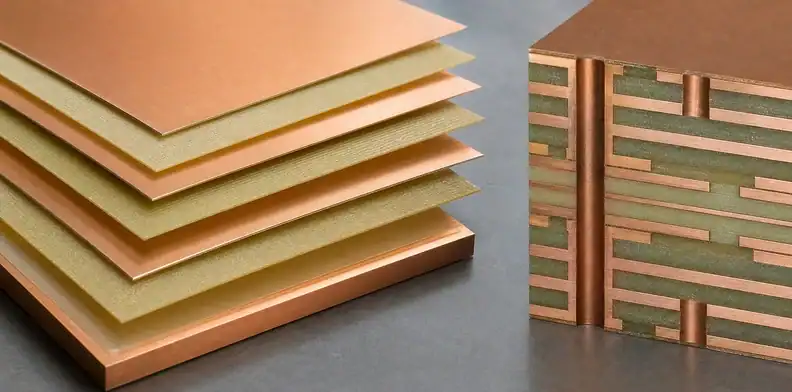
A core is a fully cured dielectric sheet, normally copper-clad on one or both sides, with a defined starting thickness and construction. A prepreg is partially cured resin and reinforcement that flows and cures during lamination. It fills copper topography, bonds layers, and becomes a finished dielectric only after the fabricator’s press cycle.
That manufacturing difference matters to electrical design. A core table may describe a known cured thickness and glass construction. A prepreg selection must be evaluated for its post-lamination thickness, resin distribution, and compatibility with the adjacent copper pattern. Calling both layers by one laminate family can hide the variables that a field solver and CAM engineer need to know.
The distinction is particularly important on controlled-impedance layers. A design may use a core dielectric in one location and a pressed prepreg dielectric in another. Their nominal Dk, glass style, and thickness can differ even before manufacturing variation is considered. The stack-up needs to show each layer independently.
Construction rule: Treat core and prepreg as separate specified objects, even when they come from the same material family.
Why resin content changes electrical behavior
Glass reinforcement and resin contribute differently to the behavior of a dielectric layer. Resin content influences the effective dielectric properties, the response to heat and pressure, and the ability of prepreg to fill copper features. A resin-rich construction can therefore behave differently from a glass-rich construction with the same product-family name.
This does not mean the buyer must calculate every resin-flow detail alone. It means the supplier should identify the actual construction used around critical layers and state the assumed pressed thickness. That gives the design owner enough information to decide whether the field-solver model and the quoted board describe the same structure.
| Layer question | Why it matters | Evidence to request |
|---|---|---|
| Is it core or prepreg? | Defines whether the dielectric is already cured or will press | Stack-up layer description |
| Which glass style is used? | Changes reinforcement and local electrical behavior | Material construction code |
| What is the resin content or pressed result? | Influences final dielectric response and fill | Supplier press-out assumption |
| Which copper layers surround it? | Determines flow and finished thickness | Copper weights and pattern context |
Resin content also belongs in a high-speed discussion because it can affect the local dielectric environment around a signal. For a published explanation of dielectric construction and stack-up trade-offs, use the prepreg construction reference. The two topics meet at the finished construction, but one is not a replacement for the other.
Layer check: A resin-content comparison is meaningful only after the intended core or prepreg construction is named.
How press-out changes impedance geometry
Impedance is sensitive to conductor geometry and dielectric height. Prepreg press-out changes the separation between a signal trace and its reference plane, which can change impedance even when the trace artwork does not move. The board designer may calculate a nominal geometry from a catalog thickness; the fabricator needs a construction that produces the intended finished dielectric after lamination.
Copper pattern matters because resin flows around it. A dense plane, a sparse signal area, a heavy copper region, and a large etched opening do not present the same lamination condition. If the design has critical impedance layers next to unusual copper distribution, the supplier should identify whether the proposed press-out remains suitable and whether a stack-up adjustment is required.
This is why a finished stack-up is more valuable than a raw bill of materials. The layer-order and reference-plane article explains how reference planes and layer order support signal integrity. Add finished dielectric values to that structure before routing dimensions are locked.
Avoid a false precision trap. A supplier cannot responsibly promise an exact pressed thickness without understanding copper pattern and build method. The proper response is a controlled range, an approved stack-up, and a process or coupon plan that matches project risk.
Modeling check: Recalculate a controlled line when an approved core or prepreg construction changes, even if the material family name remains unchanged.
Which stack-up layers need exact construction callouts
Not every dielectric layer needs the same level of control. Start with layers adjacent to impedance-controlled traces, high-speed differential pairs, RF lines, fine-pitch BGA escape regions, and structures where dielectric thickness also controls via geometry. These layers need named core or prepreg constructions, target pressed thickness, and an approval boundary for substitutions.
Power and mechanical layers can still matter. A thick core may set the whole board thickness and influence drilling aspect ratio. A buildup prepreg may determine whether a microvia reaches its target pad correctly. In an HDI design, the same layer description can affect both impedance and sequential-lamination feasibility.
The HDI stack-up types article is useful where the core/prepreg choice interacts with build-up structure. Do not assume a standard multilayer construction is viable after microvias and sequential lamination are added.
Approval point: Name the construction wherever a thickness or dielectric change would require new trace geometry, new via geometry, or fresh signal-integrity approval.
How copper distribution affects lamination assumptions
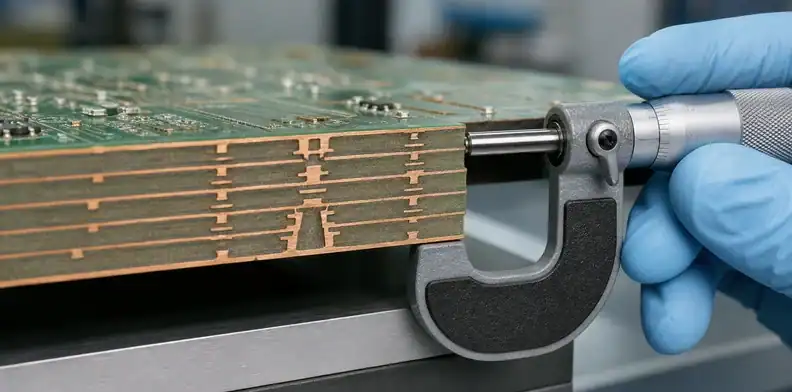
Copper distribution changes how prepreg flows and where the dielectric settles. Large copper-free areas can allow different resin behavior from dense copper fields, while heavy copper creates topography that needs sufficient resin to fill. These effects can influence local thickness, planarity, registration, and impedance consistency.
The buyer does not need to impose a universal resin-flow note on every board. Instead, identify special conditions: large copper imbalance, heavy power planes, embedded copper features, impedance-critical regions, or tightly controlled finished thickness. Give the supplier room to flag a press-out issue before production rather than after the board has been built.
Copper balance also links stack-up choice to panel design. The PCB copper balance drawing review covers how drawing information can make a potential lamination concern visible to CAM. Combine that review with an approved material table; neither document alone is enough.
If the fabricator proposes a different prepreg to improve fill, ask what it does to the finished dielectric height and electrical model. A process improvement can be acceptable, but it should not become an invisible signal-integrity change.
How to approve an equivalent material without losing control
An equivalent material proposal should be assessed by construction, not marketing category. Ask the supplier to identify the replacement core or prepreg, its glass style, nominal and finished thickness, relevant electrical data, and the layers affected. Then determine whether trace widths, pair spacing, loss assumptions, or microvia geometry must change.
For an early prototype, a controlled equivalent may be enough when the goal is mechanical fit or assembly learning. For a channel-critical or production release, an alternate should go through the same stack-up and evidence review as the original material. A lower cost is not proof that the alternate is electrically interchangeable.
The PCB material substitution approval process gives a structure for recording the technical reason, the affected revision, and the required sign-off. Use it before an alternate material reaches a released purchase order.
The same approach protects design reuse. A previous board may have used a core and prepreg combination successfully, but a new board can change copper balance, finished thickness, high-speed layers, or BGA escape density. Reusing the material name without reviewing those differences can turn a known construction into an untested one. Reuse the evidence, then confirm that the new layer geometry remains within its scope.
At quotation stage, ask the supplier to distinguish “available from stock” from “approved for this construction.” Stock availability describes procurement. Approval requires the proposed layer table, press-out assumptions, and any routing changes to be visible to the design owner.
| Layer role | Construction risk | Release field |
|---|---|---|
| Impedance signal layer | Pressed height differs from the model | Finished dielectric thickness |
| BGA buildup | Resin fill and via landing margin interact | Prepreg construction and buildup sequence |
| Thick power region | Copper topography changes local press-out | Copper pattern assumption |
What belongs in a stack-up sign-off package
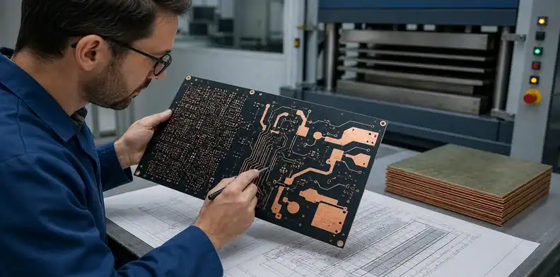
Use the table as a cross-functional handoff, not merely an engineering attachment. Purchasing needs enough detail to spot a quote that replaces a named prepreg. CAM needs enough detail to recognize which layers are electrically controlled. Quality needs the same revision when comparing first-article evidence to later builds. A construction table that serves all three roles is far less likely to be weakened during order transfer.
A sign-off package should show the layer sequence, each core and prepreg construction, finished copper, target pressed dielectric thickness, impedance-controlled layers, and any allowed alternative. Include the drawing revision, material data-sheet revision where relevant, and the owner who can approve a change. This turns a fabrication question into a traceable engineering decision.
For controlled lines, add the target impedance, geometry, reference plane, and expected evidence such as a coupon or supplier calculation. For an HDI board, add the buildup sequence and microvia spans. For an assembly-sensitive board, state thickness and flatness constraints that affect component fit. The package should be understandable by design, CAM, purchasing, and quality without relying on email history.
The sign-off should also define what is allowed to vary. A supplier may be permitted to use an approved equivalent within a named family, or every core/prepreg substitution may require a revised table. Put the rule in the document instead of relying on a buyer to remember an earlier email. This is especially valuable when a repeat order moves to a second source or returns after a long gap.
Before release, perform one final consistency check: every impedance-critical layer in the drawing should be traceable to a core or prepreg entry in the approved table. Every entry should have a material designation, finished thickness assumption, adjacent copper condition, and an approval owner. Missing one of those fields is a reason to reopen the stack-up, not a reason to hope CAM will infer it.
A useful drawing note can reference the approved stack-up instead of reproducing every construction code. It should say that the controlled table governs material build and that any core, prepreg, or pressed-dielectric change requires written approval. This leaves the release package readable while preserving the technical boundary.
QueenEMS can review a proposed stack-up when you provide the layer table, critical nets or interfaces, copper distribution concerns, planned material family, and any alternate under consideration. The review can identify information that needs agreement before a quote becomes a production construction. Submit the package through the QueenEMS contact page.
FAQ
Can I use the same Dk for core and prepreg from one material family?
Not automatically. Use the value and construction applicable to the layer being modeled, then confirm the finished pressed result with the fabricator.
Does prepreg thickness stay the same after lamination?
No. Prepreg changes during the press cycle. The finished dielectric thickness depends on the material, copper pattern, layer construction, and fabrication process.
Is a core always more stable than prepreg for impedance?
No. A core begins as a defined cured sheet, but the final impedance still depends on finished copper, adjacent layers, and the full stack-up. Both require a controlled construction.
What should I approve before a material substitute is used?
Approve the revised stack-up. It should state the affected core or prepreg, finished dielectric impact, geometry impact, and the person responsible for the release decision.
Sources
- IPC, Base Material Consideration for High Speed Printed Circuit Boards
- IPC, High Frequency Dk and Df Test Methods Comparison
Written by the QueenEMS Engineering Team
Upload your files today · Free DFM check before production · Ship worldwide
Get your PCB prototypes in as fast as 24 hours. We handle FR4, Rogers, and hybrid boards up to 40 layers in volume production, with advanced builds subject to engineering review — free prototypes for 2–4 layer FR-4 boards, no minimum order.
Just upload your Gerber + BOM — we source every part, assemble, and inspect (AOI + X‑Ray) so you don't have to chase suppliers. Boards ship in as fast as 24 hours.