
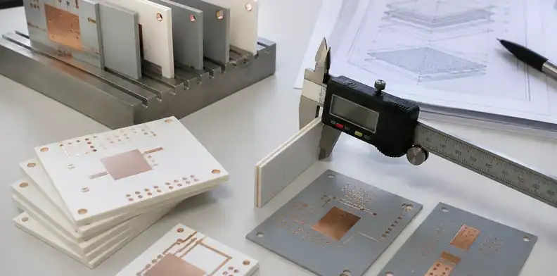
Ceramic PCB thickness, copper thickness, and trace/space capability are often quoted as simple numbers. In real sourcing work, those numbers only make sense after the supplier knows the ceramic material, metallization route, copper bonding process, hole structure, finish, and whether the order is prototype or repeat production.
That is why overseas buyers can receive very different answers from Chinese ceramic substrate suppliers for the same drawing. One factory may read the file as a thin-film alumina circuit. Another may quote it as DPC on AlN. A power module supplier may treat the same request as DBC or AMB, where copper thickness and routing rules are governed by a very different manufacturing route.
Quick Answer: There is no single standard ceramic PCB thickness. As published product-family examples, the Rogers curamik data sheet lists DBC on 0.63 mm alumina with 0.127 or 0.3 mm copper, and AMB on 0.32 mm silicon nitride with 0.5 or 0.8 mm copper. These are Rogers examples, not QueenEMS capability promises. Specify ceramic core, copper construction, finished thickness and controlled datum separately; then confirm trace/space, holes, finish and inspection for that exact material and process combination.
For general PCB terminology, see standard PCB board thickness, copper thickness comparisons and trace width and spacing. In a ceramic drawing, state the ceramic grade and conductor process before applying those dimensions.
Table of Contents
- What should ceramic PCB thickness mean in an RFQ?
- How do ceramic routes change thickness and copper limits?
- Why is copper weight the wrong question for some ceramic boards?
- What trace and space capability should buyers ask for?
- How do vias, cavities, slots, and finish change the answer?
- What should a supplier capability table include?
- When should prototype and production rules differ?
- How should overseas buyers compare quotes?
- What files should you send for capability review?
What should ceramic PCB thickness mean in an RFQ?
Ceramic PCB thickness should mean the controlled thickness of each functional layer: ceramic core, copper or metallization, dielectric or insulating layers if used, finish, and any cavity or recess feature. A finished total thickness alone is not enough for a supplier to judge manufacturability.
For alumina and AlN substrates, the ceramic plate thickness may drive heat path, stiffness, package height, impedance geometry, and assembly handling. For DBC and AMB substrates, bonded copper thickness also changes the mechanical and thermal stress picture. For LTCC, the fired ceramic stack and buried features matter more than a single board-like dimension.
A buyer’s RFQ should separate target thickness from negotiable thickness. The drawing can state the nominal finished thickness, but the quote package should identify which dimension is critical. Package height, screw clamping, optical alignment, heat-sink contact, and RF impedance may all use thickness differently.
| Thickness field | What the buyer should clarify |
|---|---|
| Ceramic core thickness | Material, tolerance, flatness need, and whether substitution is allowed |
| Copper or metallization thickness | Bonded copper, plated copper, thick film, thin film, or DPC route |
| Finished total thickness | Inspection basis and whether finish is included |
| Local recess or cavity depth | Datum, tolerance, and affected component area |
| Assembly height limit | Whether solder, die attach, TIM, or package lid must be included |
The practical question is not “can you make this thickness?” It is “which thickness controls the product, and which dimensions can the supplier adjust without changing the design intent?”
How do ceramic routes change thickness and copper limits?
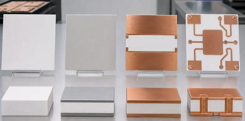
Keep material and process in separate fields. Alumina and AlN identify ceramic materials; DBC, AMB, DPC, thick film and thin film identify conductor or bonding routes. LTCC describes a co-fired multilayer ceramic construction with its own material system and design rules.
See the Ceramic PCB Guide for the relationship between DBC, DPC, AMB, and substrate choice, then put the finished thickness and copper geometry into the capability review.
An alumina thin-film circuit can support different line geometry than a thick-film ceramic circuit. A DBC or AMB substrate can carry heavier copper for power modules, but that does not mean it will match fine signal-line spacing. LTCC can integrate multilayer ceramic features, but its conductor, via, shrinkage, and design-rule assumptions must be reviewed with the supplier before layout is treated as transferable.
The QueenEMS ceramic PCB manufacturer hub gives the broader sourcing context. For this article, the key point is narrower: choose the route first, then ask thickness, copper, and trace/space questions inside that route.
| Ceramic route | Thickness and copper implication | Capability question |
|---|---|---|
| Alumina circuit | Common for insulating ceramic substrates and sensor/LED/RF carriers | Which metallization route and tolerance apply? |
| AlN circuit | Used when heat spreading matters more | Can the supplier hold thickness, flatness, and copper adhesion for the heat path? |
| DBC | Direct bonded copper on ceramic for power substrates | What copper thickness and isolation geometry are standard for this process? |
| AMB | Active metal brazed copper on ceramic for demanding power modules | What edge clearance, copper pattern, and stress rules apply? |
| DPC | Plated copper on ceramic, often used where finer patterns are needed | What line/space, via, and plating limits are controlled? |
| LTCC | Multilayer fired ceramic with internal conductors | What fired-shrinkage and buried-feature rules control the layout? |
Changing from DPC to DBC, or from thin film to thick film, is not a pricing adjustment. It can change the usable conductor geometry, heat path, soldering behavior, and inspection evidence.
Why is copper weight the wrong question for some ceramic boards?
Copper weight is useful for many FR-4 PCBs, but it can be misleading for ceramic PCB sourcing. Ceramic substrates may use bonded copper, plated copper, thick-film metallization, thin-film metallization, or multilayer fired conductors. These routes do not all map cleanly to the same “oz copper” language.
For DBC and AMB, copper thickness is usually discussed as bonded copper or copper layer thickness, because the copper sheet and ceramic bond are part of the substrate system. For DPC, the buyer may need to discuss plated copper thickness, via metallization, and finish. For thin-film or thick-film ceramic circuits, conductor material and deposition route may be more important than an FR-4 copper-weight comparison.
The older QueenEMS copper article is still useful for current density and general PCB language. For ceramic work, use that knowledge as a translation aid, then ask the supplier to quote the real ceramic construction.
Translate common PCB wording into ceramic construction language. Instead of “use 2 oz copper,” ask for the conductor thickness required for the selected ceramic route and current path. Instead of “heavy copper ceramic PCB,” ask whether the quote is DBC, AMB, DPC, plated copper, or thick-film metallization. A note such as “same copper as the FR-4 board” should trigger review of current, heat, soldering, and line/space before the supplier chooses a ceramic route.
Copper thickness also affects spacing. Thicker copper may need more generous pattern geometry, edge clearance, solder mask or no-solder-mask assumptions, and stronger stress review.
What trace and space capability should buyers ask for?
Trace/space capability should be requested as a process-qualified geometry for the selected ceramic route, copper thickness, finish, and production quantity. A bare minimum line/space number does not tell the buyer whether the design is safe for yield, inspection, soldering, or repeat orders.
For signal and RF ceramic circuits, trace geometry may control impedance, resonance, coupling, and loss. For power ceramic substrates, isolation spacing, copper edge geometry, creepage, solder area, and thermal stress may matter more than the smallest printable trace. For mixed-signal modules, both sides of that discussion can appear on the same substrate.
Ask the supplier to classify each critical feature as standard, requiring engineering review, prototype-only or not recommended. Agree what those labels mean for the quoted construction; they are review categories, not industry certification levels.
| Capability level | What it means in sourcing |
|---|---|
| Standard | Suitable for normal quote, repeatability, and fewer CAM questions |
| Engineering review | Possible only after stackup, panel, copper, via, and finish review |
| Prototype only | May be acceptable for a test coupon but risky for production transfer |
| Not recommended | Should trigger redesign or route change before quoting |
Line/space should also be tied to inspection. Ask whether the supplier will inspect by AOI, microscope, dimensional report, coupon, or another method appropriate for the route. Without an inspection basis, a small geometry number is just a marketing claim.
A Published Copper–Geometry Combination
The 2026 Rogers curamik product information and data sheet lists the following examples. Its geometry table is labelled typical width of / spacing between conductors. These are product-family design data, not QueenEMS capability commitments or rules for every ceramic process.
| Construction shown in the source | Copper thickness | Listed conductor width / spacing |
|---|---|---|
| DBC on 0.63 mm alumina | 0.127 mm | ≥0.35 mm |
| DBC on 0.63 mm alumina | 0.3 mm | ≥0.5 mm |
| AMB on 0.32 mm silicon nitride | 0.5 mm | ≥0.7 mm |
| AMB on 0.32 mm silicon nitride | 0.8 mm | ≥1.0 mm |
The thickness-combination table and geometry table must both permit the design. A fine line quoted for thin copper cannot simply be retained when the copper gets thicker. Before ordering through QueenEMS, confirm the selected material grade, ceramic and copper tolerances, finished-versus-artwork dimensions, local etch geometry, inspection method and whether the quoted facility supports that exact combination.
How do vias, cavities, slots, and finish change the answer?
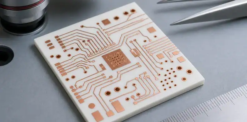
Vias, cavities, slots, and surface finish can make an otherwise acceptable ceramic PCB thickness or trace/space request difficult. These features change the local ceramic strength, metallization coverage, plating path, assembly clearance, and inspection plan.
A via in alumina or AlN is not the same sourcing question as a plated through-hole in FR-4. The buyer should identify whether the via is electrical, thermal, filled, capped, laser-formed, mechanically drilled, or part of a multilayer ceramic route. Each choice affects tolerance, yield, and whether the supplier can safely quote the design.
Cavities and slots add another control layer. A cavity may be needed for die placement, optical alignment, package height, or thermal contact. Slots may serve isolation or mechanical clearance. Both can concentrate stress in brittle ceramic, so they must be reviewed with copper spacing, edge distance, and assembly force in mind.
Finish also changes manufacturability. ENIG, silver, nickel/gold, solderable pads, wire-bondable surfaces, and die-attach surfaces may require different metallization assumptions. A design that is easy with one finish may become difficult or unsuitable with another.
Relevant DFM details belong in the drawing. The ceramic PCB design rules article is the better place for layout rules. In this capability article, the buyer’s task is to keep feature geometry tied to the chosen process route.
What should a supplier capability table include?
A supplier capability table should describe the route being quoted, not a generic ceramic PCB menu. The table should make clear what the supplier considers standard, what needs engineering review, and what is outside the quoted process.
Useful capability responses include material family, ceramic thickness range, conductor route, conductor thickness basis, trace/space level, minimum hole or via assumptions, slot/cavity notes, finish options, tolerance basis, inspection evidence, and prototype-to-production transfer conditions.
The buyer should also ask for exception handling. A supplier may be able to build one aggressive feature, but not in combination with thick copper, tight flatness, cavities, and short lead time. Combination risk is where many ceramic RFQs become unclear.
| Capability field | Acceptable supplier response |
|---|---|
| Ceramic material and route | Alumina, AlN, LTCC, DBC, AMB, DPC, thick film, or thin film stated clearly |
| Thickness basis | Core, copper, finish, and finished total separated |
| Conductor basis | Plated, bonded, printed, fired, or deposited route stated |
| Line/space basis | Standard vs review-only and tied to copper/finish |
| Hole or via basis | Formation method, metallization, and inspection expectation |
| Production transfer | Whether the prototype rule can be used for repeat builds |
The response should not hide behind “according to factory capability.” That phrase does not tell engineering what can be released, what must be redesigned, or what purchasing is actually buying.
When should prototype and production rules differ?
A prototype can include a documented exception for electrical learning, fit or material comparison. That exception is not permission to relax safety or the acceptance criteria required for the test. Before repeat production, confirm that the feature can be manufactured and inspected consistently, or revise it through an approved design change.
Imagine a prototype whose package height is acceptable, followed by a production quote offering thinner ceramic and thicker copper while keeping the same total thickness. This illustrative substitution can look harmless in the purchasing summary. The first check is the dimensional datum: does the assembly locate the part from its ceramic face, its backside metal or the finished mounting surface? Equal overall height does not necessarily preserve the die-attach surface or cavity relationship.
Mark the original and proposed layer boundaries on one cross-section. Recalculate the dimensions that reach the mating component, including their allowed variation. Then check the revised copper build against the supplier’s line-and-space rule for that combination. A proposal can fit the enclosure and still invalidate a narrow gap; conversely, widening a conductor may disturb a component land even when the spacing is acceptable.
Request a first-article report that measures the controlled mounting and attachment surfaces as well as overall thickness. Compare the difficult conductor features with their finished drawing limits and trial the mating hardware without forcing the substrate into position. If the quote supplies only total thickness, leave the substitution unresolved. Production transfer requires the individual layers and their functional dimensions to agree, not merely the sum shown on a calliper.
For early prototypes, ask the supplier to label features as standard, review-only, or prototype-only. For production, ask which features should be widened, moved, simplified, or converted to a different ceramic route. That discussion is more useful before production pricing than after a pilot lot is late.
The QueenEMS page on ceramic PCB maximum size limitations is related because size, thickness, and flatness often move together. Larger ceramic panels can make the same thickness or trace rule harder to hold.
How should overseas buyers compare quotes?
Overseas buyers should compare ceramic PCB quotes by route, controlled dimensions, process assumptions, evidence, and communication quality. Price alone is not meaningful when one supplier quotes DPC, another quotes DBC, and a third quote does not state how copper or trace/space will be controlled.
A good comparison matrix separates material and process first. Then it compares thickness tolerance, conductor route, line/space level, via or cavity assumptions, finish, inspection evidence, lead time, and what requires engineering approval. The lowest price may still be the wrong quote if it changes the ceramic route or weakens documentation.
| Quote comparison item | Why it matters |
|---|---|
| Route named clearly | Prevents DPC, DBC, AMB, LTCC, and thin-film options from being mixed |
| Thickness definition | Shows whether the supplier understands the product datum |
| Copper definition | Prevents FR-4 copper-weight language from hiding ceramic construction |
| Trace/space basis | Shows whether geometry is standard, review-only, or prototype-only |
| Evidence package | Gives engineering and quality something to approve |
| English DFM response | Reduces delay for US, CA, EU, and IL teams working across time zones |
Documentation is part of the capability. Overseas teams need DFM comments, material notes, inspection reports, and revision questions in English so hardware, quality, and purchasing can approve the same record.
When asking QueenEMS to coordinate a prototype or low-volume order, specify the required English DFM response, manufacturing scope and inspection deliverables. The quotation should identify which party fabricates the ceramic and which party supplies assembly or test evidence.
What files should you send for capability review?
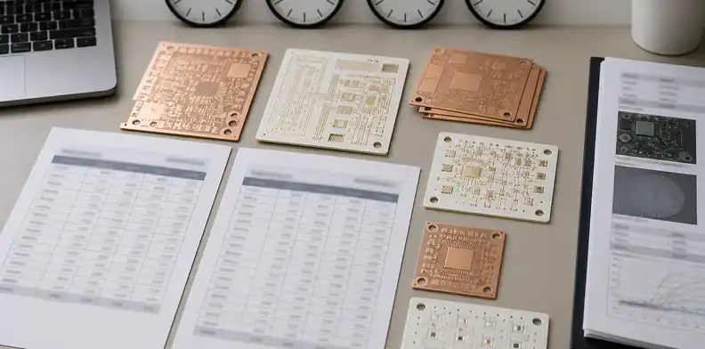
Send enough files for the supplier to review the actual manufacturing route, not only a sales inquiry. A ceramic PCB thickness or trace/space answer becomes much stronger when the supplier sees the drawing, Gerber or ODB++ data, stackup, current path, thermal requirement, finish, assembly method, and quantity stage.
The RFQ should also identify what is flexible. Purchasing may be able to accept a different ceramic thickness, but engineering may not be able to accept a changed cavity depth. Copper thickness may be adjustable on a heater board but fixed on a power module. Trace width may be tunable for DC routing but locked for RF impedance.
A short RFQ sentence can prevent long delays:
Please review this ceramic PCB stackup for manufacturable thickness, conductor route, copper thickness, trace/space, via/cavity rules, finish, and prototype-to-production transfer risk. Mark each exception as standard, engineering review, prototype-only, or not recommended.
For supplier selection beyond one drawing, the QueenEMS article on ceramic supplier qualification checks gives a broader checklist. Use this page when the immediate question is whether a specific ceramic drawing fits a supplier’s real process.
Send QueenEMS a ceramic PCB capability review package
Submit the drawing for a thickness and geometry review. Include the ceramic grade, copper stack, finished thickness datums, smallest conductors, interconnect details and package-height limits. Ask for each exception to be marked on the drawing, with its effect on assembly and the quoted inspection method.
FAQ
What is the standard ceramic PCB thickness?
There is no single standard ceramic PCB thickness that fits every project. The useful answer depends on alumina vs AlN vs LTCC vs DBC/AMB/DPC route, finished thickness tolerance, flatness, copper or metallization thickness, and assembly height.
Can ceramic PCBs use 1 oz or 2 oz copper?
Some ceramic routes can be discussed in copper-thickness terms, but many should be quoted by conductor route instead. Ask whether the supplier is quoting bonded copper, plated copper, thick-film, thin-film, or fired metallization before comparing the number to FR-4 copper weight.
Are fine traces possible on ceramic PCB?
Fine traces can be possible on suitable ceramic routes, but the safe line/space depends on material, conductor process, thickness, finish, inspection, and whether the order is prototype or production. Ask for standard, engineering-review, and prototype-only capability levels.
Why did two ceramic suppliers give different trace/space answers?
They may be quoting different processes. A DBC or AMB power substrate, a DPC ceramic PCB, a thin-film alumina circuit, and an LTCC module have different geometry assumptions even when the drawing looks similar.
Should I send a drawing before asking for capability?
Yes. A drawing, stackup, Gerbers or ODB++ files, finish notes, and controlled-dimension list make the answer much more reliable than asking for a generic line/space chart.
Sources
- Kyocera, Fine Ceramic Package and Substrate Technologies
- Rogers, curamik Ceramic Substrates Product Information and Data Sheet (2026)
Written by the QueenEMS Engineering Team
Upload your files today · Free DFM check before production · Ship worldwide
Get your PCB prototypes in as fast as 24 hours. We handle FR4, Rogers, and Flex up to 60 layers — free prototypes for 2–4 layer boards, no minimum order.
Just upload your Gerber + BOM — we source every part, assemble, and inspect (AOI + X‑Ray) so you don't have to chase suppliers. Boards ship in as fast as 24 hours.