
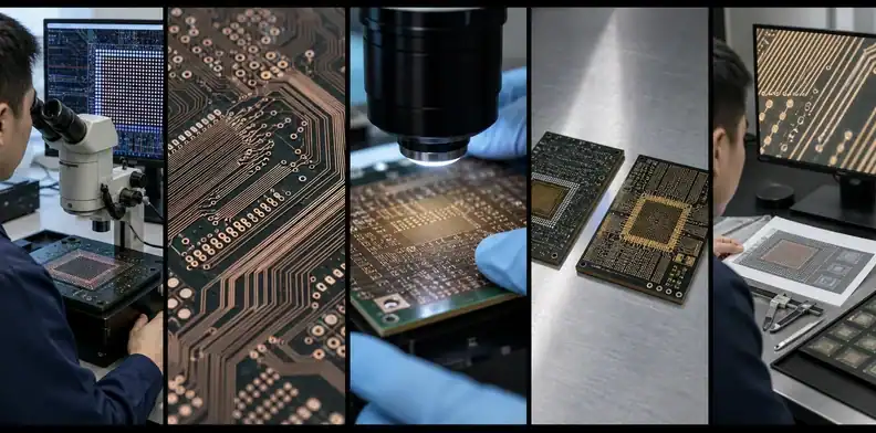
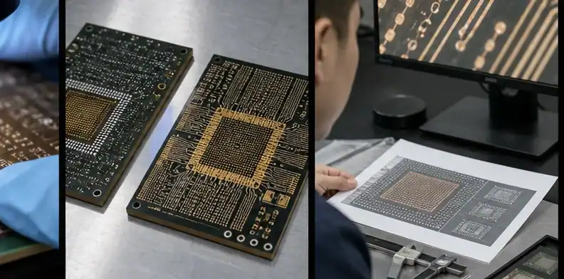
Quick Answer: BT fine-line and fine-pitch capability depends on the material reinforcement, copper process, laser microvia control, supplier class, and yield target. Many BT package substrates can support fine routing with mSAP or related processes, but ultra-fine sub-10 micrometer redistribution usually pushes the design toward ABF, silicon interposer, glass core, or another higher-density package route.
Key takeaways
- BT is stronger than ordinary FR-4 for many package-substrate routing needs, but it is not the same as ABF for the finest features.
- Glass reinforcement helps mechanical stability yet limits the most aggressive laser and fine-line geometry.
- mSAP and SAP can improve line/space, but yield and cost change quickly as features shrink.
- The RFQ should state line/space, pad pitch, microvia size, capture pads, copper thickness, and inspection evidence.
Designers often ask how fine BT can go. The honest answer is that the limit is not one number. It depends on the supplier’s process route, copper thickness, panel size, material family, microvia structure, and yield expectation. This article focuses on BT substrate capability boundaries, not general HDI routing rules. To place this decision beside related material, application, and sourcing questions, use the complete BT PCB resource as the hub page.
| Feature target | BT implication | Buyer action |
|---|---|---|
| 30/30 micrometer class | Often practical | Confirm production capability |
| 20/20 micrometer class | Supplier-dependent | Ask process route and yield |
| Sub-10 micrometer class | Usually beyond BT | Review ABF or another route |
| Limiting feature | What to ask | Possible design response |
|---|---|---|
| Microvia capture | Diameter and pad evidence | Larger pad or staggered via |
| Line/space | Routine capability | Extra layer or wider trace |
| Finish clearance | Pad function | Adjust mask or finish notes |
Table of Contents
- What line and space can BT achieve?
- What is the finest pitch on BT substrate?
- How glass fiber limits BT fine features
- BT vs ABF for ultra-fine lines
- How mSAP enables finer BT routing
- Yield and cost trade-offs of going finer
- What to send for a fine-pitch BT quote
- How to compare fine-pitch BT quotes
What line and space can BT achieve?
BT line and space capability can range from relatively standard fine PCB geometry to package-substrate class routing, depending on the process. In buyer discussions, practical BT capability is often discussed around 30/30 micrometer, 20/20 micrometer, and more advanced targets for selected suppliers. A quoted number is not useful without copper thickness, inspection method, yield expectation, and whether the process is subtractive, SAP, or mSAP. Capability signal: Ask for routine production line/space, not only the supplier’s best-case demonstration number.
What is the finest pitch on BT substrate?
The finest pitch on BT substrate depends on pad type, attach method, escape routing, microvia size, and layer count. A fine-pitch BGA, CSP, flip-chip, or sensor package may all use BT, but each has a different routing problem. For board-style routing, QueenEMS’ fine-pitch BGA fanout page provides adjacent layout context. Pitch rule: The pad map and escape route define the BT challenge more clearly than the headline pitch alone.
How glass fiber limits BT fine features
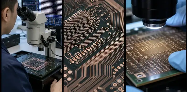
Glass fiber gives BT laminate stiffness and dimensional control, but it also limits the most aggressive fine features. Laser drilling, dielectric uniformity, and fine copper formation can be affected by glass weave and resin distribution. This limitation is not a defect; it is a material boundary. Material boundary: Glass reinforcement helps BT behave as a stable organic substrate, while also setting a practical floor for fine-feature scaling.
BT vs ABF for ultra-fine lines
BT and ABF should not be compared only by cost. ABF is used for very high-density package substrates because its build-up film supports finer redistribution than many reinforced BT routes. BT remains attractive where routing density is moderate, cost matters, and package construction benefits from mature organic laminate. The BT versus ABF fine-line limits article covers the wider substrate comparison. Selection rule: Use BT when the feature set fits mature package-substrate routing; move beyond BT when escape density is the main driver.
How mSAP enables finer BT routing
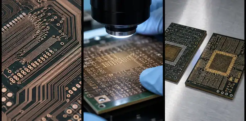
mSAP enables finer BT routing by using a semi-additive copper process rather than relying only on subtractive etching from thicker foil. This can support tighter lines and spaces with better control, especially in package and SLP-style work. The relationship between BT, HDI and SLP helps place this decision. Process call: mSAP is useful only when the supplier can tie it to the required line/space, copper thickness, and yield plan.
Yield and cost trade-offs of going finer
Yield and cost change quickly as BT features become finer. Narrower copper raises etch or plating sensitivity, smaller microvias tighten registration, and dense pads reduce repair margin. The supplier may need stricter inspection, slower processing, special material, or lower panel utilization. The cost of finer features article explains how these details show up in pricing. Price rule: Fine BT routing should be justified by package need, because every tighter feature spends yield margin.
What to send for a fine-pitch BT quote
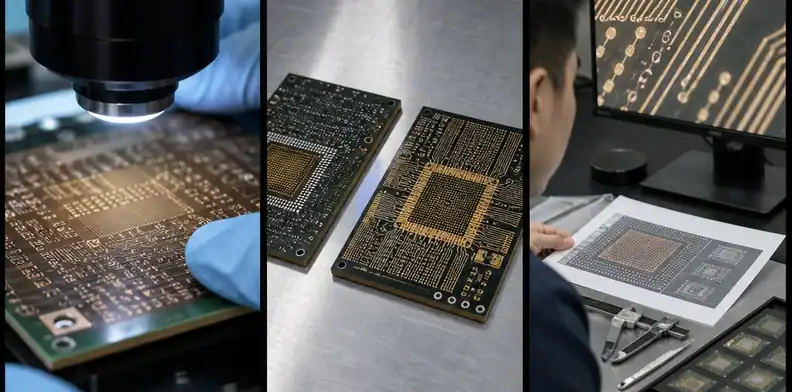
Send Gerber or ODB++ files, pad map, BGA or die pitch, line/space target, copper thickness, microvia size, capture pad, layer count, stack-up, finish, impedance or RF notes, and quantity stages. Mark which features are fixed by the package and which can be adjusted during DFM. Keep the pad map, stack-up, and limiting geometry in the same RFQ packet so capability is judged against the real escape route rather than an isolated line-width number.
Extra buyer notes for capability claims
Capability tables can mislead when they mix prototype, pilot, and mature production limits. A supplier may show a very fine line width from a demonstration coupon, while the actual order needs higher yield, larger panels, controlled finish, and repeat lots. Buyers should ask for routine production capability for the selected material, copper thickness, and panel class.
The routing escape should be reviewed before the quote is treated as final. A fine-pitch BGA or die pad map may require more layers, smaller vias, or a different process route. If the supplier quietly changes capture pads or line width assumptions, the electrical design may no longer match the package intent. Mark critical geometry in the RFQ so DFM suggestions do not become unauthorized design changes.
Microvia reliability matters as features shrink. The quote should state whether vias are stacked, staggered, filled, plated over, or capped, and whether cross-section evidence is included. A small via diameter without plating evidence is not enough for a high-reliability package.
Cost comparison should use the same geometry. One supplier quoting 30/30 micrometer with a stable process and another quoting 20/20 micrometer with engineering review are not comparable. Ask each supplier to identify which feature drives cost and which relaxation would improve yield.
Fine-pitch escape planning should include the package body, not only the inner pad field. A BGA or die array may escape cleanly near the center but fail near corners, shields, keepouts, or test pads. Ask the supplier to mark the actual congestion point so engineering knows whether the bottleneck is line width, via capture, layer count, or finish clearance.
Copper thickness can change the answer. A line/space value that is reasonable with thin copper may become difficult with thicker copper. If the design needs current carrying, low resistance, or special finish thickness, the fine-line capability should be reviewed with those requirements included.
Inspection resolution should be part of the quote. Very fine copper needs AOI, dimensional checks, and sometimes cross-section or microsection evidence around microvias. A supplier that can fabricate a feature but cannot inspect it consistently may not be the right production path.
Supplier geography and volume also matter. Some shops can prototype aggressive geometry but cannot support repeat volume or schedule predictability. For small overseas buyers, it is often better to choose a slightly more relaxed geometry that several qualified suppliers can support than to depend on one narrow process window.
The design owner should define which lines are functionally critical. RF paths, impedance-controlled traces, and escape routes may have different tolerance sensitivity. If every line is treated as equally critical, the quote becomes harder to optimize; if critical nets are marked, the supplier can focus evidence where it matters.
Fine-pitch design review before RFQ release
Start the review with the pad field. Count how many rows must escape, where ground and power pins sit, and which signals require controlled length or impedance. The supplier cannot judge BT capability from nominal pitch alone. The escape pattern reveals whether the design needs finer lines, smaller microvias, extra layers, or a different package substrate.
Next, separate production features from prototype experiments. A prototype may accept lower yield and manual engineering attention. Production needs a geometry that can be inspected, repeated, and priced predictably. Ask the supplier which feature they would relax first if the build had to move from prototype to repeat production.
Then check copper and finish together. Fine lines with thin copper may be feasible, while the same spaces with thicker copper or a demanding finish may become harder. If the package needs ENEPIG, wire-bond pads, or tight solder mask definition, the finish decision should be included in the fine-line review.
Microvia stacking also deserves attention. Stacked vias, via-in-pad, filled vias, and capped vias can solve routing problems but add process and reliability requirements. A supplier quote should state whether these vias are standard for the proposed BT route and what evidence is included.
For supplier comparison, ask each factory to identify the single most limiting feature. One may point to line width, another to microvia capture, another to panel registration. Those answers are more useful than a yes/no capability claim because they show what engineering can change to improve yield.
Capability evidence buyers can request
For fine-line BT, ask for a capability answer tied to your exact copper thickness. A factory may support a tight line/space with thin copper but not with the copper weight or plated finish your package needs. This one question often explains why quotes differ.
Ask whether the supplier will inspect critical features on the production panel or only rely on a general process capability statement. Dense BT substrates may need AOI, dimensional measurement, or microsection evidence around the most sensitive vias and traces.
Ask whether the design has any feature below routine capability. If yes, request a first-article or pilot condition rather than pretending the feature is ordinary production. That keeps engineering aware of yield risk and prevents purchasing from treating all quotes as equal.
Ask what relaxation would improve yield. The answer might be wider line/space, larger capture pad, staggered microvias, one more layer, or changed copper thickness. A supplier who can name the best relaxation is giving useful engineering input, not merely selling capacity.
How to avoid over-specifying fine lines
Many designs ask for finer line/space than they truly need because the first layout was routed under pressure. Before locking the BT RFQ, engineering should check whether one extra layer, a different escape direction, or a slightly larger package would relax the tightest area. A small layout change can save more cost than supplier negotiation.
The buyer should also split critical and noncritical geometry. Some traces carry RF, clock, or high-speed signals; others are ordinary escape routes. If the supplier sees which features are critical, it can focus inspection and DFM effort on the right locations.
When a supplier proposes a relaxation, ask for the engineering consequence. Wider lines may affect impedance, larger pads may affect capacitance, and shifted vias may affect escape density. The right answer is not always to accept the easier feature; the right answer is to know what changes.
For production planning, record the accepted fine-line class. That way a later repeat order does not get requoted with a different process route simply because a new buyer used a different description.
The final design review should include assembly clearances. Fine BT routing may be manufacturable, yet the finished package can still fail if solder mask, finish, probe access, or bonding clearance is too tight. A supplier that reviews only copper width may miss the assembly conflict. Send the package drawing and attach method with the routing files so capability is judged in context.
For quote comparison, ask suppliers to quote the same inspection scope. A low price without fine-feature inspection can look attractive until the assembler finds opens, shorts, or weak vias. A slightly higher quote that includes evidence for the limiting geometry may be cheaper than debugging an undocumented failure after delivery.
The buyer should also preserve the final CAM interpretation. If the supplier approves a fine-line adjustment, store the accepted line width, spacing, pad change, or via change with the released package. Future orders then reuse a controlled decision rather than rediscovering the same routing limit.
How to compare fine-pitch BT quotes
Compare fine-pitch quotes by routine line/space, microvia evidence, copper thickness, and whether the supplier marks any feature as engineering review. The smallest number is not automatically the best production route.
Send the pad escape map, line/space target, microvia plan, copper thickness, finish, impedance notes, and quantity stage via QueenEMS engineering contact. The fine-pitch BT routing review can then separate routine production features from geometry that should move to a more advanced substrate path.
FAQ
What line and space can BT do?
It depends on supplier and process route. Many practical BT package discussions fall around 30/30 micrometer to 20/20 micrometer classes, with tighter targets requiring review.
Is BT better than FR-4 for fine pitch?
Yes for many package-substrate and SLP-style needs, because BT supports thinner, more stable organic package builds than ordinary FR-4.
Why does glass fiber limit BT?
Glass reinforcement helps stiffness and dimensional control, but it can limit the smallest laser microvias and finest redistribution features.
When do I need ABF instead?
Consider ABF when routing density, escape pitch, or sub-10 micrometer class redistribution exceeds practical BT capability.
Sources
- Mitsubishi Gas Chemical, Low-CTE BT resin laminate lineup
- Global Electronics Association, IPC-6921 organic IC substrate standard
Written by the QueenEMS Engineering Team
Upload your files today · Free DFM check before production · Ship worldwide
Get your PCB prototypes in as fast as 24 hours. We handle FR4, Rogers, and Flex up to 60 layers — free prototypes for 2–4 layer boards, no minimum order.
Just upload your Gerber + BOM — we source every part, assemble, and inspect (AOI + X‑Ray) so you don't have to chase suppliers. Boards ship in as fast as 24 hours.