
You finished your high-power schematic and need to test a thermal management solution, but ordering a ceramic board is fundamentally different from a quick-turn FR4 run. Hardware engineers consistently waste thousands of dollars and lose weeks of development time because they blindly submit standard Gerber files to ceramic manufacturers without specifying critical high-temperature bonding parameters. To successfully order your first ceramic PCB prototype, you must submit specialized material specifications, understand the required tooling costs, and expect a 7-to-15 day fabrication cycle.
Quick Answer: Ordering a ceramic PCB prototype requires submitting exact substrate purity levels (e.g., 96% Alumina) and specific metallization processes (like DBC or AMB) alongside your standard Gerber files. Because factories must run dedicated high-temperature furnace cycles, a 5-piece prototype batch typically costs $50 to $200 per board with an average lead time of 7 to 15 days, entirely unlike a standard 24-hour FR4 service. Key takeaways:
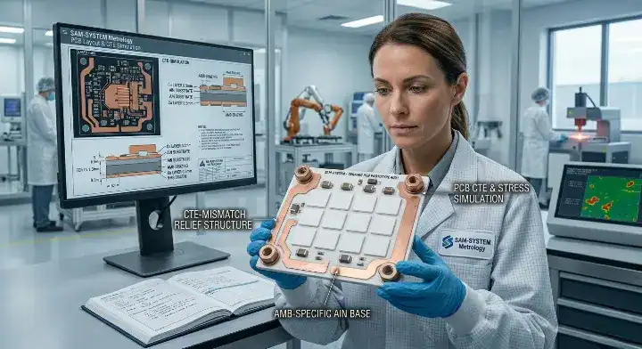
- Do not submit a standard FR4 quote request; ceramic boards require explicit copper thickness callouts for Direct Bonded Copper (DBC) processes.
- Aluminum Nitride (AlN) prototypes cost 5 to 8 times more than standard Alumina (Al2O3).
- You must request a minimum 0.3mm trace-to-edge spacing to prevent the ceramic from shattering during laser depanelization.
- A 5-piece order incurs fixed NRE tooling costs ($200-$500), making the unit price significantly higher than mass production rates.
Table of Contents
- 1. Why Do Ceramic PCB Prototypes Cost So Much More Than FR4?
- 2. What Files Do Ceramic Manufacturers Actually Need for a Quote?
- 3. What Are the 5 Most Common Mistakes First-Time Buyers Make?
- 4. Do You Actually Need a Ceramic Prototype, or Will MCPCB Work?
- 5. Which Ceramic Manufacturing Process Fits Your Design?
- 6. How Do You Choose Between Alumina and Aluminum Nitride for Testing?
- 7. Why Does a Ceramic Prototype Take 7 to 15 Days to Build?
- 8. What Specific DFM Constraints Apply Only to Ceramic Boards?
- 9. What Should You Measure During Your First Article Inspection?
- 10. How Can You Reduce the Cost of Your First Prototype Run?
1. Why Do Ceramic PCB Prototypes Cost So Much More Than FR4?
A 5-piece ceramic PCB prototype batch typically costs $50 to $200 per board because you must absorb the fixed $200-$500 Non-Recurring Engineering (NRE) tooling fees and high-temperature furnace operating costs over a tiny production volume. In mass production runs of 10,000 units, these exact same boards drop drastically to $3 to $15 per unit.
Non-Recurring Engineering (NRE) fees are fixed, one-time charges covering the creation of specialized laser cutting programs and custom high-temperature furnace fixtures, typically averaging $300 for a standard ceramic layout.
Engineers ordering for the first time routinely experience sticker shock. When you run 5 boards through a 1,065°C furnace cycle, the energy and setup costs remain identical to running 500 boards.
Calculate the true cost structure:
- Raw Alumina material costs 3x more than FR4 paneling.
- Laser cutting machine time charges out at a premium rate.
- Fixed setup costs heavily distort low-volume unit pricing.
Bottom line: Stop comparing ceramic prototype pricing to FR4; budget an upfront $500 to $1,000 to cover the fixed tooling and setup costs for your initial 5-to-10 piece trial run.
2. What Files Do Ceramic Manufacturers Actually Need for a Quote?
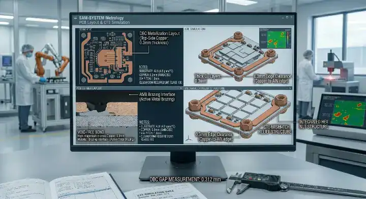
Ceramic manufacturers require a comprehensive specification sheet detailing the exact substrate material purity, the required metallization process, and specific dielectric test voltages, alongside your standard RS-274X Gerber files. Submitting a bare FR4-style Gerber package without these mechanical callouts forces the factory to reject your RFQ or delay your quote by an entire week.
First-time buyers constantly complain on engineering forums about sending files to a ceramic PCB manufacturer and receiving endless clarifying questions instead of a price quote. The factory physically cannot quote your design without knowing how to bond the copper.
A medical startup submitted a basic FR4 Gerber file for an AlN prototype and lost 8 days answering email inquiries about copper thickness. We provided them with our standard ceramic RFQ checklist. The client re-submitted their next revision with complete material and process callouts, receiving an accurate, ready-to-build quote in under 4 hours.
| Required Specification | Standard FR4 File | Ceramic Prototype File |
|---|---|---|
| Substrate Callout | “FR4 High-Tg” | “96% Alumina (24 W/m·K)” |
| Copper Bonding | “1oz Copper” | “DBC, 140µm Copper” |
| Edge Clearance | “0.1mm” | “0.3mm Minimum” |
If you are requesting a quote for standard FR4, a basic Gerber zip file is sufficient. If you are ordering a ceramic prototype, you must attach a detailed mechanical drawing specifying the exact ceramic grade and metallization method.
Bottom line: Attach a PDF mechanical drawing to your Gerber files explicitly listing your required substrate purity (e.g., 96% Al2O3) and metallization type (e.g., DBC).
3. What Are the 5 Most Common Mistakes First-Time Buyers Make?
First-time buyers destroy their prototyping budget by requesting unrealistic ±0.05mm dimensional tolerances that ceramic materials physically cannot hold during the laser cutting process. A standard ceramic laser cutter maintains a strict ±0.1mm tolerance, meaning tighter specifications simply cause the factory to instantly reject the design for manufacturing violations.
Review this immediate failure checklist:
- Mistake 1: Specifying standard copper weights (1oz) without explicitly naming the Direct Bonded Copper (DBC) process.
- Mistake 2: Requesting non-standard substrate thicknesses (like 1.0mm) instead of standard 0.635mm sizes.
- Mistake 3: Demanding physical dimensional tolerances tighter than ±0.1mm.
- Mistake 4: Designing plated through-holes (PTH) on a DBC board, which requires DPC instead.
- Mistake 5: Failing to request a blank test coupon for internal qualification testing.
Bottom line: Design your prototype using a standard 0.635mm thickness and a ±0.1mm dimensional tolerance to guarantee the factory can physically manufacture your board.
4. Do You Actually Need a Ceramic Prototype, or Will MCPCB Work?
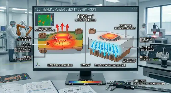
You absolutely need a ceramic prototype if your component power density exceeds 10W/cm² or if your operating junction temperature consistently spikes above 150°C. If your thermal load remains under 8W/cm², a high-end Metal Core PCB (MCPCB) utilizing a 3.0 W/m·K dielectric layer provides a highly reliable and much cheaper thermal solution.
A 3.0 W/m·K dielectric layer is a highly thermally conductive insulating film used in advanced MCPCBs, transferring heat roughly 10 times faster than standard FR4 epoxy glass.
Determine your exact thermal boundary:
- MCPCBs choke under extreme currents because the required dielectric insulating layer blocks rapid heat transfer to the aluminum base.
- Ceramic substrates remove the dielectric layer entirely, bonding copper directly to an inorganic, high-conduction core.
An automotive lighting client requested a $2,500 Alumina prototype run for a simple 5W LED array. Our engineers ran a Free DFM review and proved their thermal load was only 4W/cm². We guided them back to a standard metal core PCB, slashing their prototype budget to $400 while keeping junction temperatures perfectly safe at 85°C.
| Substrate | Max Power Density | Dielectric Bottleneck | Relative Cost |
|---|---|---|---|
| MCPCB (3 W/m·K) | 8 W/cm² | Yes (Thin film) | Low ($) |
| Alumina Ceramic | 50 W/cm² | None | Medium ($$) |
If your power module pushes past 10W/cm², you must choose a ceramic substrate. If your design stays below 8W/cm², choose an advanced MCPCB to save your prototyping budget.
Bottom line: Calculate the exact power density of your hottest component; only upgrade to a ceramic prototype if that value strictly exceeds 10W/cm².
5. Which Ceramic Manufacturing Process Fits Your Design?
Direct Bonded Copper (DBC) perfectly fits heavy industrial power modules requiring thick 140µm to 300µm copper layers for massive current carrying capacity. Direct Plated Copper (DPC) fits high-frequency RF designs and high-density interconnects requiring extremely precise ±5% copper thickness tolerances and fine-pitch routing down to 50µm trace widths.
Direct Bonded Copper (DBC) is a high-temperature process melting copper foil directly onto bare ceramic at 1,065°C, providing extreme peel strength (50+ N/mm) for heavy automotive applications.
Understand the clear separation of capabilities:
- Use DBC for high current: Motor drives, solar inverters, and heavy relays.
- Use DPC for high precision: RF antennas, medical sensors, and fine-pitch LEDs.
- Use AMB for maximum reliability: You must use Active Metal Brazing (AMB) if you select Silicon Nitride (Si3N4) for extreme mechanical vibration environments.
Bottom line: Specify the DBC process for heavy power applications over 50 Amps, and specify the DPC process for complex RF layouts requiring fine 50µm traces.
6. How Do You Choose Between Alumina and Aluminum Nitride for Testing?
You choose standard Alumina (Al2O3) for 90% of industrial power modules because it delivers 24 W/m·K thermal conductivity at a highly economical price point. You only choose Aluminum Nitride (AlN) when your bare silicon die demands an exact Coefficient of Thermal Expansion (CTE) match of 4.5 ppm/°C or extreme heat extraction above 170 W/m·K.
Aluminum Nitride (AlN) prototypes cost 5 to 8 times more than standard Alumina prototypes because AlN raw material synthesis requires highly complex, non-toxic handling procedures in a controlled atmosphere.
Consider the harsh financial reality of material selection:
- A 5-piece Alumina prototype batch might cost $600.
- The exact same 5-piece layout in Aluminum Nitride will likely cost $3,500+.
| Ceramic Material | Thermal Conductivity | CTE (ppm/°C) | Relative Cost |
|---|---|---|---|
| 96% Alumina (Al2O3) | 24 W/m·K | 7.0 | Base (1x) |
| Aluminum Nitride (AlN) | 170-230 W/m·K | 4.5 | High (5x – 8x) |
If you are building a commercial LED driver, choose standard 96% Alumina. If you are building a mission-critical military laser diode requiring massive heat extraction, pay the premium for Aluminum Nitride.
Bottom line: Start your initial prototype testing with cost-effective 96% Alumina, upgrading to expensive Aluminum Nitride only if physical thermal testing proves 24 W/m·K is insufficient.
7. Why Does a Ceramic Prototype Take 7 to 15 Days to Build?
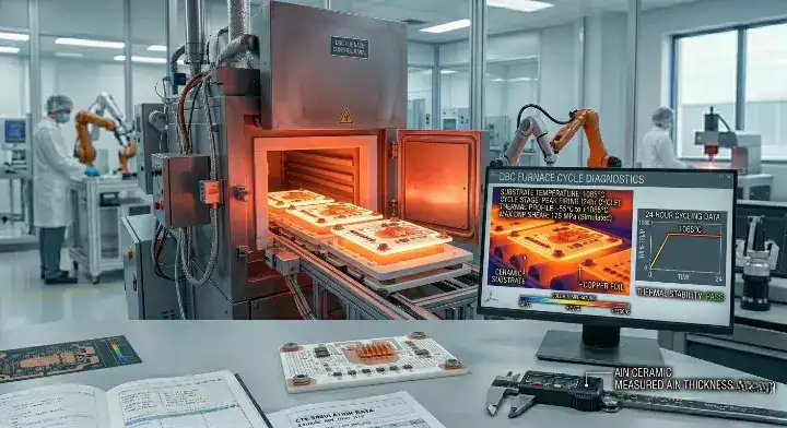
A true ceramic prototype physically requires 7 to 15 days to manufacture because the DBC bonding process mandates a slow, 24-hour high-temperature firing cycle at 1,065°C followed by a controlled cooling phase to prevent the panel from cracking. You cannot safely compress this thermodynamic process into a 24-hour “quick-turn” cycle like standard FR4 fabrication.
When you order a PCB prototype, factories throw FR4 panels into rapid chemical etching tanks. Ceramic requires entirely different thermal physics.
Here is the exact timeline breakdown:
- Days 1-2: Laser cutting the bare ceramic panel.
- Days 3-5: Chemical cleaning, copper placement, and 24-hour furnace firing.
- Days 6-8: Chemical etching of the bonded copper.
- Days 9-10: Surface finish application (e.g., ENIG) and high-voltage testing.
Bottom line: Never trust a supplier promising a custom DBC ceramic prototype in 24 hours; schedule a strict 14-day window in your project timeline for proper fabrication.
8. What Specific DFM Constraints Apply Only to Ceramic Boards?
Ceramic boards feature brittle physical characteristics requiring a minimum 0.3mm clearance between any copper trace and the laser-cut edge of the panel to prevent microscopic fractures during final separation. Designers who apply standard 0.1mm FR4 edge-spacing rules will find their ceramic prototypes physically shattering when the factory attempts to break them out of the production panel.
A hardware engineer complained heavily on the Stack Exchange forum that their manufacturer refused to build their ceramic layout. The root cause was entirely DFM-related: they placed plated through-holes on a DBC design and violated minimum hole sizes.
A telecom client submitted a dense ceramic PCB vs FR4 transition design with 0.15mm laser drill holes on a DBC layout. Our Free DFM system flagged this immediately. We educated the client that DBC requires a minimum 0.3mm hole diameter. The client adjusted the vias, and the resulting prototype run achieved a perfect 100% mechanical yield.
| Design Parameter | Standard FR4 Limit | Ceramic (DBC) Limit |
|---|---|---|
| Trace to Edge Clearance | 0.15 mm | 0.30 mm Minimum |
| Minimum Hole Diameter | 0.10 mm (Laser) | 0.30 mm Minimum |
| Plated Through Holes | Standard | Extremely Difficult |
For prototype runs (5–10 boards): expect strict adherence to 0.3mm spacing rules to guarantee the initial build. For high-volume production (1,000+ boards): expect to widen these tolerances even further to optimize factory yield rates.
Bottom line: Run a strict Design Rule Check (DRC) enforcing a 0.3mm trace-to-edge clearance and a 0.3mm minimum hole size before exporting your final Gerber files.
9. What Should You Measure During Your First Article Inspection?
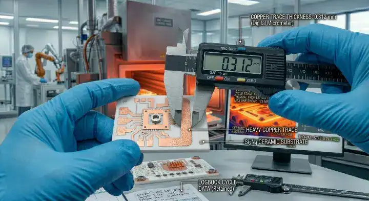
You must measure the final copper thickness using a calibrated micrometer and perform a high-voltage dielectric breakdown test to verify the prototype matches your exact mechanical specifications. A basic visual inspection cannot detect if the factory substituted a cheaper 1oz copper foil instead of your specified 140µm heavy copper requirement.
First Article Inspection (FAI) is a strict validation process where the engineering team physically measures and tests the first manufactured batch against the original mechanical drawings before approving mass production.
Execute this specific 3-point inspection plan:
- Copper verification: Measure the traces to guarantee the factory hit the ±10% DBC thickness tolerance.
- Acoustic testing: Request a Scanning Acoustic Microscopy (SAM) report to prove the bond is void-free.
- High-voltage test: Apply 2,000V DC to confirm the bare ceramic isolation remains intact.
Bottom line: Physically measure the copper trace thickness with a micrometer on the very first day you receive the prototype box to catch unauthorized factory material substitutions.
10. How Can You Reduce the Cost of Your First Prototype Run?
You reduce the cost of your first prototype run by rigidly adhering to the factory’s standard material stock sizes, specifically selecting 96% Alumina at a 0.635mm thickness. Demanding a custom 1.0mm thickness forces the factory to special-order the raw ceramic panel, instantly adding $300 to $500 to your bill and delaying your project by two weeks.
We manufacture complex power systems using the advanced ceramic PCB manufacturing process every day. The difference between an affordable prototype and a budget-destroying one is always standardization.
Follow these exact cost-reduction rules:
- Material: Use 96% Alumina, not 99% Alumina or AlN.
- Thickness: Specify exactly 0.635mm (25 mil).
- Metallization: Select standard 1oz (35µm) or 2oz (70µm) copper foil.
- Surface Finish: Use standard ENIG instead of pure soft gold wire-bondable finishes.
Bottom line: Explicitly specify 0.635mm 96% Alumina with ENIG surface finish to bypass custom material surcharges and keep your first prototype run under $600.
Ordering a ceramic prototype demands a higher level of engineering precision than buying a cheap FR4 board online. You must specify the exact metallization process, strictly follow brittle-material DFM constraints, and physically verify the finished copper thickness to guarantee your thermal tests provide valid data. QueenEMS specializes in high-power substrates, offering Free DFM reviews, 3D AOI inspection, and full turnkey service from initial ceramic prototypes to mass production. If you need to validate a heavy copper DBC design without wasting your prototyping budget, reach out via our contact us page for an expert engineering review.
Written by the QueenEMS Engineering Team
FAQ
Can I order a ceramic PCB prototype with a 24-hour lead time? No, a genuine ceramic prototype physically requires 7 to 15 days because the Direct Bonded Copper (DBC) process mandates a 24-hour high-temperature firing cycle at 1,065°C. The slow heating and cooling phases are strictly required to prevent the ceramic substrate from shattering.
What is the minimum order quantity (MOQ) for a ceramic prototype? The standard Minimum Order Quantity (MOQ) for a ceramic prototype is typically 5 pieces. While you can technically order a single board, you will still pay the exact same $200-$500 NRE tooling and furnace setup fee, making a 5-piece run the most economically viable starting point.
Why did my factory reject my plated through-hole (PTH) design? Factories reject PTH designs on Direct Bonded Copper (DBC) layouts because the DBC process melts flat copper foil onto the surface, which cannot flow down inside a drilled hole. If your design requires plated vias connecting the top and bottom layers, you must specify the Direct Plated Copper (DPC) process instead.
How do I specify the substrate material for a ceramic quote? You must specify the substrate by its exact chemical composition and purity level on your mechanical drawing. Do not write “Ceramic”; you must explicitly write “96% Alumina (Al2O3)” or “Aluminum Nitride (AlN)” so the factory can calculate the correct raw material cost.
Is Aluminum Nitride worth the extra prototype cost? Yes, it is worth the extra cost only if your design mounts a large bare silicon die directly to the board and you need an exact CTE match of 4.5 ppm/°C. If you are just testing standard packaged SMDs for thermal dissipation, stick to much cheaper Alumina.
Upload your files today · Free DFM check before production · Ship worldwide
Get your PCB prototypes in as fast as 24 hours. We handle FR4, Rogers, and Flex up to 60 layers — free prototypes for 2–4 layer boards, no minimum order.
Just upload your Gerber + BOM — we source every part, assemble, and inspect (AOI + X‑Ray) so you don't have to chase suppliers. Boards ship in as fast as 24 hours.