
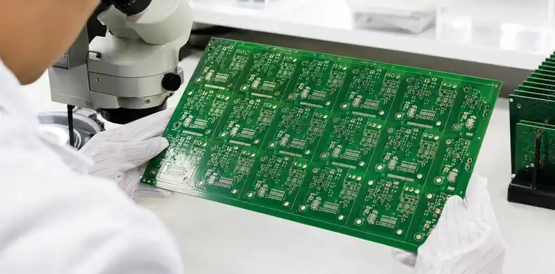
Quick Answer: Accept a lead-free HASL PCB only after the alloy requirement, complete solder coverage, finished-hole condition, pad flatness risk, laminate heat compatibility, and solderability evidence match the released assembly plan. HASL does not need to look as flat as ENIG, but uneven coating must not obstruct component seating, paste printing, holes, or the agreed workmanship criteria.
Key takeaways – The BOM and land geometry determine whether HASL topography is tolerable. – Inspect coverage, wetting, exposed copper, dewetting, solder balls, and reduced component holes. – Lead-free HASL adds a severe fabrication heat excursion that thin or complex boards must survive. – Quotes must state alloy, finish process, acceptance evidence, and any package-driven exclusion.
Lead-free HASL PCB finish remains useful for robust solderability and cost-sensitive fabrication, especially on through-hole and larger-feature assemblies. The acceptance mistake is expecting one rule to cover every layout. Molten solder is applied and levelled by air knives, so the finished coating can vary with pad geometry, board orientation, hole pattern, alloy, and process setup.
The existing HASL and ENIG comparison owns the broad finish-selection question. This page begins after lead-free HASL is proposed and asks whether the design, quotation, delivered boards, and assembly process support that choice without hidden flatness or thermal risk.
Table of Contents
- Start with the component and land map
- Specify alloy and finish scope
- Judge pad flatness by assembly risk
- Inspect coverage, wetting, and holes
- Review the laminate heat excursion
- Choose meaningful lot evidence
- Align fabrication with assembly approval
- Resolve a marginal HASL shipment
- Prepare a quote-ready HASL package
Start with the component and land map
The BOM and pad geometry decide whether lead-free HASL is a sensible production finish. Through-hole connectors, large discrete parts, test jigs, power boards, and hand-soldered prototypes often tolerate its surface profile, while tight stencil gasketing and low-standoff leadless packages need closer review.
Do not use a universal pitch cutoff as a substitute for assembly engineering. HASL equipment, orientation, land size, pad aspect ratio, stencil design, paste, package coplanarity, and process capability all influence the result. Search results often claim that every BGA or QFN automatically requires ENIG; that rule is too absolute to become a drawing requirement without checking the actual package and assembler capability.
Mark the finish-sensitive locations on the assembly drawing or review package. Small perimeter lands, large thermal pads beside tiny leads, fine-pitch gull-wing components, area arrays, bottom-terminated components, edge contacts, press-fit zones, and dense via-in-pad regions deserve individual disposition. A board may use HASL successfully over most of its area yet need an alternate or selective finish in one functional zone.
The assembler should participate before fabrication release. A fabricator can confirm whether it can coat the board, but it cannot unilaterally decide the acceptable paste-printing window or package seating for the customer’s line. Purchasing needs a single decision that both PCB and PCBA suppliers understand.
Buyer call: Approve HASL from the worst finish-sensitive land and package, not from the average pad on the board.
Specify alloy and finish scope
The drawing should say lead-free HASL and identify the required alloy or governing customer specification when composition is controlled. “Lead free” alone may not establish which solder alloy, impurity limits, or compliance evidence the program expects.
Common lead-free HASL systems use tin-based alloys such as tin-copper or stabilised variants. The buyer should not assume that every supplier runs the same bath. Alloy affects process temperature, wetting behaviour, appearance, compatibility with the assembly alloy, and the declaration included with the shipment.
Define whether the finish covers all exposed solderable copper and whether any fingers, contacts, carbon ink, selective gold, or unsoldered mechanical areas require another treatment. Mixed-finish boards need a sequence and mask plan that the fabricator can review before pricing.
The quote should also distinguish HASL from solder fusing or other tin coating language. This prevents a purchasing shorthand from producing a different process. State the required surface-finish note in the fabrication drawing and repeat the alloy requirement in the PO only when the document system needs both.
| RFQ item | Question the supplier must answer |
|---|---|
| Lead-free alloy | Which qualified bath composition is quoted? |
| Coverage | Which exposed copper areas receive HASL? |
| Selective zones | Are contacts or special pads excluded? |
| Compliance record | What alloy or material declaration ships with the lot? |
| Change control | Does an alloy or process-site change require approval? |
The table prevents two suppliers from quoting different lead-free systems under the same three-letter finish name.
Judge pad flatness by assembly risk
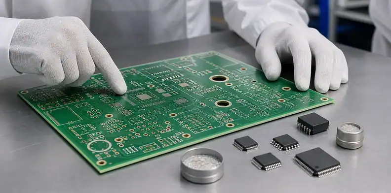
HASL flatness is acceptable when the finished pad profile still supports stencil contact, solder-paste volume, component seating, and joint formation for the actual assembly. It should not be judged by comparing its surface visually with a chemically deposited planar finish.
Air knives remove excess molten solder, but pad size and orientation can leave variable thickness or a domed profile. On large through-hole lands, that topography may create no practical problem. On a fine-pitch leaded package, one raised land can affect paste transfer or lead contact. On a bottom-terminated component, the interaction between perimeter pads and a large exposed pad deserves review.
Use the PCB drawing and BOM together. Identify minimum lead pitch, package standoff, stencil thickness, thermal-pad geometry, placement tolerance, and whether solder-paste inspection is available. An assembler with mature HASL experience may accept a geometry that another line rejects, which means supplier capability must be part of the release decision.
Flatness requirements should be measurable when they are contractually important. Avoid a note such as “pads must be perfectly flat”; no fabrication process delivers a mathematical plane. Instead, define the component-driven concern, agreed inspection method, sample plan, or approved finish alternative.
The wider surface-finish measurement article explains report control. For HASL, the useful question is often profile variation across representative lands rather than one nominal coating value.
Flatness boundary: A cosmetically uneven pad may pass, but a profile that disrupts printing or seating on a controlled package does not.
Inspect coverage, wetting, and holes
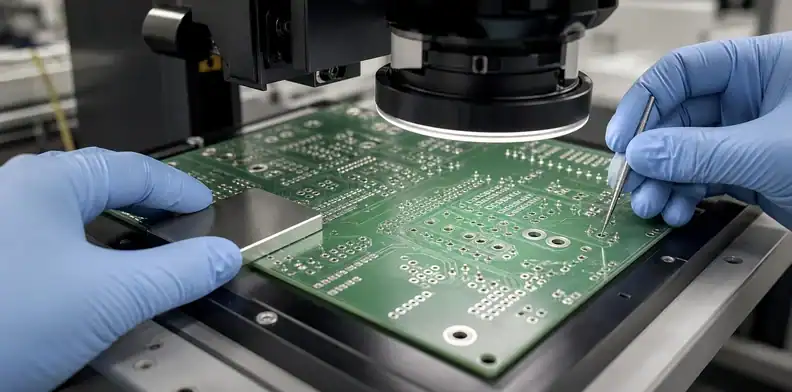
Delivered boards should show complete solder coverage on required exposed copper, acceptable wetting, no prohibited dewetting or nonwetting, no exposed copper where finish is required, and no solder obstruction that reduces a component hole below its finished-size requirement.
Inspect several feature types instead of only the easiest large pads. Include small lands, large copper areas, plated-through component holes, dense connectors, isolated pads, board edges, and locations that faced the air-knife direction. Look for solder balls, icicles, bridging, mask damage, trapped residues, rough deposits, plugged holes, and finish on areas intended to remain clear.
A bright surface is not the only acceptable appearance, and visual shine does not prove wetting. Apply the product’s workmanship standard, drawing, and approved visual samples. IPC technical literature describes good HASL surfaces as smooth and showing no evidence of nonwetting or dewetting, but the exact contract should identify the governing printed-board acceptance documents.
Finished holes need special attention because excess solder can reduce insertion clearance. Verify critical connector and lead holes against the released finished-hole range after finishing. Do not drill or mechanically clear production boards without engineering approval; that can damage hole-wall plating and invalidate acceptance.
For receiving teams, integrate these checks into the PCB incoming inspection plan with photographs, location references, sampled dimensions, and a lot hold rule.
Acceptance rule: Coverage and workmanship must pass on representative pad and hole types, not only on a convenient corner coupon.
Review the laminate heat excursion
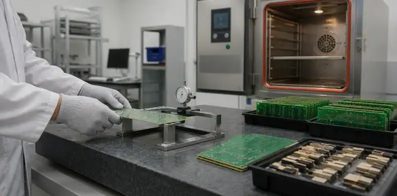
Lead-free HASL subjects the printed board to a high-temperature fabrication step, so the laminate, plated holes, sequential structures, board thickness, and copper balance must tolerate that excursion before assembly adds more cycles.
Thin boards can distort during hot-air levelling. Thick multilayers and high-aspect-ratio holes store more thermal stress. Blind vias, stacked structures, resin systems with limited decomposition margin, and boards already near a warpage limit deserve an explicit process review. The finish decision therefore reaches beyond exposed pads.
Ask the material supplier or fabricator for the laminate’s applicable lead-free process data and qualification basis. Do not infer suitability from Tg alone. Decomposition behaviour, Z-axis expansion, time above temperature, moisture condition, press construction, copper distribution, and the actual HASL profile all contribute to risk.
The design may still be suitable after review. The point is to prevent a low-cost finish choice from creating delamination, barrel stress, or bow and twist on a complex build. When the stack-up is marginal, compare a lower-temperature deposited finish and account for assembly needs rather than forcing HASL through procurement.
If flatness or bow and twist becomes the dominant concern, use the existing PCB warping cause review for panel symmetry and structural factors, then add the finish-specific heat exposure to the supplier discussion.
Release rule: High-complexity or thin constructions need laminate and via compatibility review before lead-free HASL is frozen.
Choose meaningful lot evidence
Lot evidence should prove the finish that was ordered, the workmanship conditions most likely to fail, and any controlled alloy or solderability requirement. Avoid asking for a generic certificate bundle that does not identify the production lot.
A basic package may include part and revision, lot and date code, lead-free alloy declaration, outgoing visual result, critical finished-hole measurement, and packaging record. Higher-risk orders may add solderability testing, profile or thickness measurements on agreed features, thermal-stress evidence, microsection results, or customer-source inspection.
Solderability requirements should name the test basis and trigger. A new supplier qualification, delayed assembly, suspect appearance, multiple heat exposures, or customer mandate can justify more evidence than a stable repeat order. The bare-board solderability test specification can be linked in the quality plan when wetting proof is required.
Keep measurement purpose clear. Coating thickness varies on HASL, and the thinnest and thickest pad conditions may occur on different geometries. If a report is requested, define locations and what decision the data supports. A random measurement from one large pad cannot establish fine-pitch coplanarity across the board.
| Evidence | Suitable use | Weak version |
|---|---|---|
| Alloy declaration | Confirms specified lead-free system | Generic RoHS logo |
| Visual inspection record | Coverage and workmanship release | “Appearance OK” with no sample basis |
| Finished-hole report | Protects connector insertion | Pre-finish drill chart only |
| Solderability result | Confirms wetting under named conditions | Unidentified coupon photograph |
| Thermal qualification | Supports complex laminate construction | Tg value without process context |
This evidence set should scale with risk and remain consistent between RFQ, PO, shipment, and receiving.
Align fabrication with assembly approval
Fabrication and assembly suppliers should approve the same finish-sensitive feature list before the board order is released. The PCB supplier controls coating capability and finished-board workmanship; the assembler controls stencil gasketing, paste volume, placement, package seating, and reflow performance.
Create one marked drawing or review table that identifies the smallest perimeter leads, area-array packages, exposed thermal pads, critical through holes, and any selective-finish boundaries. Ask the fabricator to state the expected HASL condition on those features and the assembler to state whether its printing and placement process can tolerate it.
| Approval owner | Question to close |
|---|---|
| PCB fabricator | Can the named alloy and process meet the marked land and hole conditions? |
| Assembler | Can stencil, paste, placement, and reflow tolerate the resulting finish profile? |
| Product engineering | Does the combined evidence support release for the intended product? |
Resolve conflicting responses through a documented engineering decision. Changing to ENIG may be appropriate, but the team can also revise a land pattern, stencil aperture, component choice, or selective finish when that better fits the product. The decision should account for bare-board cost, assembly evidence, rework accessibility, and the consequence of a hidden joint defect.
Preserve the approved component revision. A package change under the same schematic function can introduce smaller lands or lower standoff after the PCB finish has been frozen. BOM alternates therefore need a finish-compatibility check when their packages differ.
Decision rule: The finish is ready for purchasing only after the board fabricator and assembler have accepted the same critical land map.
Resolve a marginal HASL shipment
Contain a marginal shipment by bag or panel lot, document the exact feature, and separate cosmetic roughness from functional obstruction, exposed copper, poor wetting, hole-size loss, laminate damage, or assembly flatness risk.
The first response should preserve samples. Photograph a board overview and the local feature with scale; record pad type, orientation, affected quantity, lot distribution, and package condition. Measure critical holes and board flatness using the released method. Do not scrape solder, force component leads through holes, or locally reflow boards before the supplier reviews untouched evidence.
Assembly trials can be useful when geometry is the question. Choose representative components and the planned stencil, paste, and reflow process. Record solder-paste inspection and post-reflow observations instead of relying on one hand-soldered pad. A trial may support a limited deviation, but it does not rewrite the production drawing.
Possible dispositions include release, sorted release, additional testing, supplier rework, deviation for a named quantity, replacement, or rejection. The decision owner depends on the issue: assembly engineering owns print and seating risk, design engineering owns functional change, quality owns conformity, and purchasing owns the commercial settlement.
Disposition line: A use-as-is approval must identify the affected lot, package features, supporting trial or inspection, and whether the concession applies to repeat builds.

Prepare a quote-ready HASL package
A quote-ready package combines the fabrication data with the assembly conditions that make lead-free HASL acceptable. Send Gerber or ODB++, drill data, fabrication drawing, stack-up, board thickness, copper weights, finish alloy requirement, BOM package summary, minimum component pitch, critical holes, and the evidence list.
State the planned assembly sequence: hand solder, one-sided reflow, double-sided reflow, wave, selective soldering, or expected repair. Mark BGA, QFN, land-grid, fine-pitch, press-fit, and contact areas. Where the assembler has an explicit finish restriction, include it before the board supplier quotes.
A useful drawing note can say:
Apply the specified lead-free HASL alloy to all designated solderable copper. Finished pads shall meet the agreed workmanship and assembly requirements, with complete coverage and no exposed copper, prohibited dewetting, or solder obstruction of component holes. Notify the buyer before changing alloy, process site, or approved selective-finish boundaries.
Send QueenEMS the released board package, alloy requirement, finish-sensitive component list, soldering sequence, critical finished-hole table, and requested lot records through the QueenEMS quotation contact. The review can return a finish-risk disposition, clarification questions, and a quote that separates normal HASL scope from any special inspection or selective treatment.
RFQ signal: The accepted price must correspond to a named alloy, compatible board construction, known assembly geometry, and defined shipment evidence.
FAQ
Is lead-free HASL unsuitable for every BGA or QFN?
No. Risk depends on package pitch, pad geometry, HASL process, stencil design, assembler capability, and required yield. Review the actual BOM and land pattern instead of applying an unsupported universal ban.
Can I accept HASL pads that are not perfectly flat?
Yes, when the profile meets the agreed workmanship criteria and does not impair paste printing, placement, seating, or solder-joint formation. A component-driven acceptance method is better than a cosmetic demand for perfect flatness.
What should be checked in plated component holes?
Verify that solder does not plug the hole or reduce it below the specified finished diameter. Also inspect coverage, hole-wall condition where visible, and any evidence of thermal damage around the land.
Does a RoHS certificate identify the HASL alloy?
Not necessarily. RoHS compliance addresses restricted substances; the order should separately identify the required alloy or customer specification and request the relevant material declaration.
Sources
Written by the QueenEMS Engineering Team
Upload your files today · Free DFM check before production · Ship worldwide
Get your PCB prototypes in as fast as 24 hours. We handle FR4, Rogers, and hybrid boards up to 40 layers in volume production, with advanced builds subject to engineering review — free prototypes for 2–4 layer FR-4 boards, no minimum order.
Just upload your Gerber + BOM — we source every part, assemble, and inspect (AOI + X‑Ray) so you don't have to chase suppliers. Boards ship in as fast as 24 hours.