
Quick Answer: A production-ready pcb assembly drawing must include mechanical board dimensions, exact component placements with clear Pin 1 polarity indicators, and designated keep-out zones to prevent a 100% rework rate on misaligned parts. Supplying a complete drawing cuts engineering hold times by up to 3 days and eliminates the standard $5 to $15 per-board manual rework fees caused by relying solely on inaccurate silkscreen markings.
Key takeaways:
- Always mark Diodes, LEDs, and IC Pin 1 orientations directly on the drawing to prevent component reversal.
- Create separate top and bottom-side drawings for any design exceeding 50 SMT components.
- Clearly label “Do Not Populate” (DNP) components on both the BOM and the visual drawing.
- Document hatched zones for conformal coating rather than hiding instructions in email threads.
Table of Contents
- What Is a PCB Assembly Drawing and Why Does Your CM Need It?
- What Information Must Every Assembly Drawing Include?
- What Are the Most Common Assembly Drawing Mistakes CMs See?
- How Should You Mark Component Polarity and Orientation?
- When Do You Need a Separate Top-Side and Bottom-Side Drawing?
- How Do You Document Special Assembly Instructions?
- What Is the Difference Between Assembly Drawing and Fabrication Drawing?
- Assembly Drawing Quality Checklist Before Submission
- FAQ
You just spent weeks routing a high-density board, and now your contract manufacturer is delaying production to ask basic questions about component orientations. Sending bare manufacturing files without a visual blueprint forces factory operators to guess your design intentions, directly risking thousands of dollars in scrapped hardware. QueenEMS maintains a 99.7% first-pass yield rate primarily because we demand strict visual documentation before loading any job onto the SMT line. Providing a clear, dimensioned drawing eliminates operator guesswork and guarantees the factory builds your hardware exactly as engineered.
What Is a PCB Assembly Drawing and Why Does Your CM Need It?
A pcb assembly drawing is a 2D engineering blueprint that shows human operators and quality control machines exactly where to place, orient, and solder every electronic component on the bare board, reducing placement defects by up to 95%. Without this visual document, contract manufacturers cannot verify if the automated pick-and-place machine has populated the board correctly according to your specific design intent.
Many hardware designers assume that machine data is enough. While the automated equipment uses coordinate files to place parts, the human technicians running the line use the visual drawing to set up the feeders, inspect the first article, and perform manual soldering tasks. Your BOM for PCB assembly tells the factory what to buy, but the drawing tells them how to build it.
- First Article Inspection: Quality control engineers compare the first physical board directly against your PDF drawing.
- Manual Assembly: Operators rely on visual callouts to hand-solder through-hole connectors.
- Discrepancy Resolution: If the machine coordinate file conflicts with the silkscreen, the factory treats the drawing as the ultimate source of truth.
Bottom line: Treat your drawing as a binding visual contract for production; if a physical detail is not clearly visible on this document, the factory is not liable for building it incorrectly.
What Information Must Every Assembly Drawing Include?
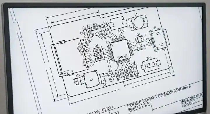
Every compliant drawing must feature a dimensioned board outline, component reference designators, distinct polarity markings, and designated keep-out areas, matching the IPC-D-326 documentation standard for printed circuit assemblies. Including these specific elements prevents pre-production engineering holds that typically delay your build schedule by 2 to 4 business days.
| Element | Required or Optional | What It Tells the CM | Common Mistakes |
|---|---|---|---|
| Board Outline | Required | Physical boundaries and mechanical fit | Missing overall X/Y dimensions |
| Reference Designators | Required | Links the physical pad to the BOM item (e.g., C1, R5) | Text too small to read at 100% zoom |
| Polarity Indicators | Required | Pin 1 location, cathode marks, connector keying | Relying entirely on the silkscreen layer |
| Mounting Holes | Required | Points of mechanical fastening | Not specifying if the hole is plated |
| DNP Labels | Required | Which specific pads must remain empty | Only marking DNP status in the BOM spreadsheet |
Comparison Anchor: If you have a simple 10-component prototype, a basic PDF showing reference designators works fine; if you have a high-density board with tight mechanical enclosures, you must include exact ASME Y14.5 tolerancing data for all edge connectors.
Bottom line: Never submit a drawing that only displays blank component outlines; you must explicitly render the reference designators and polarity dots to make the document functional on the factory floor.
What Are the Most Common Assembly Drawing Mistakes CMs See?
The most expensive error on an assembly drawing for CM is omitting IC polarity marks, which forces a 100% rework rate costing $5 to $15 per board when operators install the chips backward. The second most common mistake is failing to mark “Do Not Populate” (DNP) parts with a visual “X”, leading operators to solder expensive components onto pads that should have remained empty.
Factory Perspective: The single most expensive assembly drawing error we see is wrong polarity on ICs. Two months ago, a customer’s drawing showed a QFN-48 MCU with pin 1 in the upper-left corner, but the actual physical component had pin 1 in the lower-left. The silkscreen on the bare PCB matched the drawing—meaning both were wrong. The centroid file also contained the flawed rotation. Our operators assembled 60 boards before quality control caught the discrepancy during functional testing (every board failed to power on). The result: 60 boards × $12 rework labor = $720 in wasted cash, plus 3 days of production delay while we desoldered and re-placed every single MCU. The fix would have taken the engineer 30 seconds: verify the pin 1 orientation against the component datasheet before exporting the drawing.
- Silkscreen Discrepancies: Silkscreen ink often shifts during fabrication, obscuring polarity marks. The drawing must clarify these ambiguities.
- DNP Marking Rules: DNP (Do Not Populate) components are parts listed in the design but excluded from the current build. You must mark them on the BOM and place a visible “X” over them on the drawing.
- Missing Dimensions: Factories need overall length and width measurements to program the conveyor belt rails.
Bottom line: Always cross-reference your CAD software’s component footprints with the physical manufacturer datasheet before generating your final visual blueprints.
How Should You Mark Component Polarity and Orientation?
You must use standardized visual symbols—such as arrows for diodes, plus signs (+) for electrolytic capacitors, and solid dots for IC Pin 1—to achieve 0% orientation defects during SMT assembly. Relying purely on the physical PCB silkscreen is highly dangerous because manufacturing tolerances often cause the ink to shift by 0.1mm to 0.2mm, completely hiding the actual pad orientation under the component body.
| Component Type | Standard Marking | Drawing Notation | What Happens if Missing |
|---|---|---|---|
| Integrated Circuits (IC) | Pin 1 dot or chamfer | Solid dot next to Pad 1 | Chip installed backward, catastrophic short circuit |
| Diodes / LEDs | Cathode line | Arrow pointing to cathode | Component fails to conduct current |
| Electrolytic Capacitors | Positive terminal | Visible “+” symbol | Component explodes or bulges under power |
| Connectors | Keying notch | Outline matching physical shape | Cables cannot plug into the finished board |
Comparison Anchor: Choose a solid dot marking for dense QFN or BGA chips where space is tight; choose a full physical outline with a chamfered corner for larger SOIC or QFP packages where the body shape is distinct.
Bottom line: Visually over-communicate polarity on your drawings; a factory machine operator should never have to open your raw CAD files just to figure out which way an LED points.
When Do You Need a Separate Top-Side and Bottom-Side Drawing?
You must generate separate top-side and bottom-side drawings for any double-sided PCBA containing more than 50 total SMT components or utilizing a mixed-technology layout. Trying to overlay both sides onto a single sheet creates a tangled web of lines that reduces readability by 80% and causes severe manual inspection bottlenecks on the factory floor.
For prototype runs (1 to 10 boards) with all components placed entirely on one side, a single-page PDF is perfectly acceptable. For mid-volume runs (100+ boards) featuring double-sided placement, separating the views is a hard requirement.
- Page 1: Top-side view, scaled to fit the page, showing only top-layer components.
- Page 2: Bottom-side view, mirrored horizontally (as if flipping the physical board over), showing only bottom-layer components.
- Reference: Just like checking layers in a Gerber file guide, keeping physical layers visually distinct prevents part placement confusion.
Bottom line: Split your documentation by physical layer to match the factory’s actual manufacturing steps, printing the top view on page one and the mirrored bottom view on page two.
How Do You Document Special Assembly Instructions?
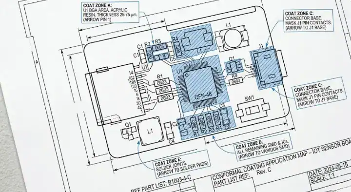
Special manufacturing instructions, such as conformal coating zones, thermal paste locations, or specific press-fit insertion forces, must be documented directly on the drawing using hatched callout boxes, preventing the 40% failure rate associated with relying on email-only communications.
| Instruction Type | Visual Example | Why It Cannot Be Verbal Only |
|---|---|---|
| Conformal Coating | Hatched zones marking “Coat Here” | Operators change across 3 shifts; verbal notes get lost |
| Thermal Paste | Shaded square under a heatsink | Missing paste causes field failures months later |
| Hand Soldering | Arrow pointing to sensitive sensor | Machines will melt the component in the reflow oven |
| Press-Fit Connectors | Text note: “Max force 50N” | Over-pressing cracks the inner layers of the PCB |
Factory Perspective: A client’s telecom board required selective conformal coating—the entire board needed coverage except for the RF antenna area and two debug connectors. This specific requirement was mentioned deep inside an email thread buried in a 15-message chain. Our production team coated the entire board on the first batch of 50 units. When the client tested them, the antenna performance was degraded by 40% due to the coating material sitting over the RF trace. We had to chemically strip and recoat all 50 boards, generating $1,500 in rework labor and a 1-week delay. After this incident, the client added a clear “conformal coating mask” layer to their drawing with hatched areas showing exactly where to coat. We have experienced zero coating errors since.
Comparison Anchor: Choose specific callout arrows for individual component instructions like press-fit connectors; choose large, hatched masking zones for area-wide treatments like potting or chemical coating.
Bottom line: If a special assembly requirement is mentioned only in an email and not printed clearly on the drawing, the contract manufacturer holds no liability for missing it during a shift change.
What Is the Difference Between Assembly Drawing and Fabrication Drawing?
A fabrication drawing dictates the physical construction of the bare printed circuit board (layer stackup, drill hole sizes, and raw materials), whereas an assembly drawing instructs the factory exactly how to populate that bare board with physical electronic components. Mixing these two completely distinct datasets onto a single file creates heavy manufacturing confusion and delays quoting processes by 24 to 48 hours.
| Feature | Fabrication Drawing | Assembly Drawing |
|---|---|---|
| Primary Purpose | How to build the bare PCB | How to solder components to the PCB |
| Core Content | Stackup, drill chart, material specs, tolerances | Part locations, reference designators, polarity |
| Who Uses It | Bare board etching facility | SMT machine operators and QC inspectors |
| Format | PDF included with Gerbers/ODB++ | PDF included with BOM and Pick-and-Place files |
Comparison Anchor: Use the fabrication drawing when communicating tolerances to the bare board chemical etching facility; use the assembly drawing when passing final placement files to the SMT line operators.
Bottom line: Keep your bare board notes and your component placement notes on strictly separate PDF documents to prevent the pick-and-place engineers from misinterpreting raw layer stackup data.
Assembly Drawing Quality Checklist Before Submission
Running your final exported PDF through a 5-point visual quality checklist—verifying outline dimensions, readable reference designators, polarity dots, DNP labels, and special instruction notes—eliminates 98% of pre-production engineering holds. A clean, standardized document package allows contract manufacturers to move your project straight to the DFM PCB design review stage without kicking files back to your desk.
Before sending your ZIP file to the factory, open your PDF viewer and perform this quick audit:
- Zoom Test: View the PDF at 100% scale. Are the reference designators legible, or are they overlapping?
- Polarity Check: Pick three random diodes and three ICs. Is the orientation obvious without opening the CAD file?
- DNP Crosscheck: Does every part marked as DNP in the BOM have a corresponding “X” on the drawing?
- Dimension Audit: Does the drawing display the overall X and Y physical dimensions of the board edge?
- Notes Verification: Are all special handling requirements (coating, masking, hand-soldering) listed in a notes block?
Bottom line: Review your exported drawing PDF at a normal zoom level before sending it out; if the text is too blurry or cluttered for you to read, the assembly line operator cannot read it either.
Frequently Asked Questions (FAQ)
What is an assembly drawing in PCB manufacturing? A PCB assembly drawing is a 2D visual blueprint used by factory operators to identify where and how electronic components should be placed and soldered onto a bare board. It displays component outlines, reference designators, and polarity marks, serving as the primary reference document for quality control inspections. Always include this PDF in your final manufacturing package.
What required elements must be on the drawing? You must include the mechanical board outline, reference designators (like R1, C2), component polarity indicators (Pin 1 dots, diode arrows), and specific keep-out zones. Missing any of these elements forces the factory to pause production and email you for clarification. Check your CAD export settings to guarantee these layers are visible.
How do you mark polarity on an assembly drawing? You use a solid dot to indicate Pin 1 on ICs, an arrow pointing to the cathode for diodes, and a clear “+” symbol for polarized capacitors. Never rely solely on the physical silkscreen text, as ink can smudge or shift during manufacturing. Add clear vector symbols to your mechanical layers before exporting the PDF.
Where should I put special assembly instructions? You must place special instructions, such as conformal coating requirements or press-fit insertion limits, directly in a text block on the drawing itself. Hiding these instructions in a separate email guarantees they will be lost during factory shift changes. Use visual hatched lines pointing to the specific areas requiring special treatment.
What is the difference between an assembly drawing and a fab drawing? The fabrication drawing contains instructions for making the bare fiberglass board (drill holes, layer stackup, copper weight), while the assembly drawing shows where to solder the physical components onto that finished board. Never mix these two documents together. Keep your fab notes in the Gerber folder and your assembly drawing with the BOM.
Providing clear, standardized documentation is the cheapest and most effective way to protect your hardware budget from avoidable rework costs. A clean assembly drawing tells the factory exactly what you expect, eliminating the guesswork that causes field failures.
QueenEMS provides a free DFM/DFA engineering review on every order. Our engineering team cross-checks your assembly drawings against your BOM and centroid files to catch polarity mismatches and missing DNP labels before the first stencil is ever cut.
Ready to build your hardware with zero orientation defects? Submit your complete file package to QueenEMS for a full turnkey quote today.
Written by the QueenEMS Engineering Team
Upload your files today · Free DFM check before production · Ship worldwide
Get your PCB prototypes in as fast as 24 hours. We handle FR4, Rogers, and Flex up to 60 layers — free prototypes for 2–4 layer boards, no minimum order.
Just upload your Gerber + BOM — we source every part, assemble, and inspect (AOI + X‑Ray) so you don't have to chase suppliers. Boards ship in as fast as 24 hours.