

Quick Answer: IPC-7095 sets the maximum bga voiding acceptable limits at 30% of the solder ball area for Class 2 and 25% for Class 3 electronics. However, relying on these upper limits often leads to thermal failures in modern high-density chips; keeping voiding strictly below 10% through optimized reflow profiles and VIPPO via treatments is the only way to guarantee long-term field reliability.
Key takeaways:
- IPC Class 3 limits BGA voiding to a maximum 25% area, but this is a process warning line, not an absolute safety guarantee.
- Unfilled via-in-pad structures increase voiding sizes by 64–74%, making copper-filled VIPPO mandatory for pitches ≤0.5mm.
- Applying 100% solder paste coverage actively traps gases; utilizing a window-pane stencil with 50–70% coverage prevents major voids.
- 2D X-Ray inspection routinely underestimates actual void volume by up to 50% due to overlapping shadows, requiring 3D CT checks.
Table of Contents
- What Is BGA Voiding and Why Should You Care About It?
- What Are the Exact IPC-7095 BGA Voiding Acceptable Limits?
- What Causes BGA Voiding in SMT Assembly?
- How Do Open Via-in-Pad Designs Create Massive BGA Voids?
- Why Does 100% Solder Paste Coverage Make Voiding Worse?
- What Reflow Profile Settings Reduce BGA Voiding Below 10%?
- Why Is 3D X-Ray the Only Reliable Way to Measure BGA Voids?
- How Do You Specify BGA Voiding Limits in Your Assembly Contract?
Does your assembly partner claim your boards pass the bga voiding acceptable limits simply because they hit exactly 25%? Factory data shows that 99.7% of critical thermal failures happen precisely because engineers treat IPC thresholds as safety targets rather than process warning signs. When volatile flux gases get trapped inside a melting joint, they create empty pockets that block heat transfer and severely weaken the mechanical bond. You need to stop accepting outdated 2D inspections and start demanding manufacturing processes that push void rates safely below 10%.
What Is BGA Voiding and Why Should You Care About It?
BGA voiding is the formation of empty gas pockets inside a solder joint during the reflow process, typically exceeding bga voiding acceptable limits when it covers more than 25% of the ball area. These voids drastically increase thermal resistance and mechanical fragility, turning minor temperature fluctuations into total connection failures.
To understand the threat, we must categorize the physical defects. A macro-void is a massive gas bubble forming within the solder bulk, often taking up 15–30% of the total joint volume. Planar microvoids sit dangerously right at the Intermetallic Compound (IMC) interface layer, creating a clean shear line where the ball will snap off under stress. Shrinkage voids happen during the rapid cooling phase. Here’s the problem: flux contains volatile compounds designed to clean oxidation, but if they vaporize and the gas bubble fails to escape before the alloy solidifies, you get a void.
- Macro-voids: Massive trapped bubbles, highly common around via-in-pad locations and large center thermal pads.
- Planar microvoids: Tiny flattened pockets sitting exactly at the IMC layer, notoriously hard to spot but deadly for mechanical shock resistance.
- Shrinkage voids: Jagged anomalies forming as the liquid metal cools and contracts unevenly.
We recently took on a client experiencing a 15% field failure rate on industrial controllers despite their previous factory showing X-Ray reports passing the 25% mark. Our engineers analyzed the boards and found heavy planar microvoids caused by moisture absorption. We instituted strict J-STD-033 baking standards for all moisture-sensitive components before reflow. The result? Field failures dropped to zero, and total void area fell to an average of 8%.
Bottom line: You cannot eliminate BGA voiding entirely, but controlling it firmly under 10% separates a reliable industrial product from a highly costly field recall.
What Are the Exact IPC-7095 BGA Voiding Acceptable Limits?
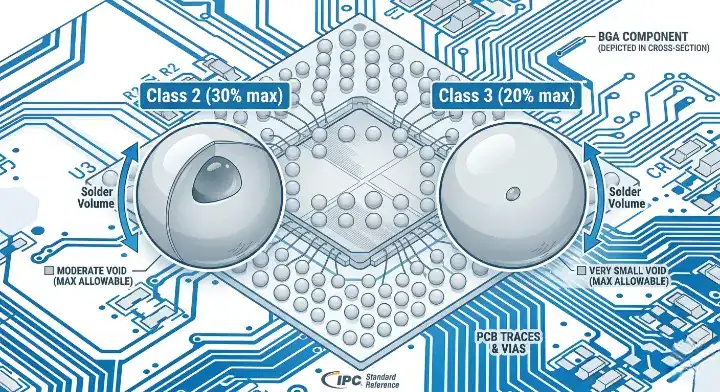
The exact bga voiding acceptable limits dictate a maximum void area of 30% for IPC Class 1 and 2, and a stricter 25% limit for Class 3 high-reliability applications. You must calculate this correctly: a void spanning 25% of the ball’s diameter only equals roughly 6.25% of its area, so always insist your factory measures area percentage to avoid massive calculation errors.
Let’s address a frequent and dangerous misconception from the ST Community Forum: “IPC-A-610G says 30% void is acceptable for my BGA, but almost every pin on my STM32 has voids near 30%. The chip overheated. Is 30% really safe?” The absolute answer is no. IPC’s 25–30% threshold is an industrial “process indicator,” not a thermal safety guarantee. A single solder ball exhibiting a 30% void might survive isolated stress. However, if 80% of the solder balls on a single BGA package hover near that 30% voiding limit, the cumulative thermal resistance skyrockets. The heat simply cannot escape the die, guaranteeing an overheating failure. The IPC standard measures a per-ball criteria, but your system’s thermal performance depends entirely on the aggregate heat path. For highly thermal-sensitive devices like MCUs, FPGAs, or power ICs, even if IPC officially allows 25%, your factory’s internal standard should be restricted to 10–15% maximum. At QueenEMS, our baseline internal standard sits strictly at voiding <10%—far exceeding IPC Class 3—and we run 100% 3D X-Ray on every thermal-critical BGA.
| Void Criteria | IPC Class 1 | IPC Class 2 | IPC Class 3 | QueenEMS Internal Standard | Notes |
|---|---|---|---|---|---|
| Max Void Area per Ball | 30% | 30% | 25% | < 10% | Area %, not diameter %. |
| Max Void in Thermal Pad | N/A | 30% | 25% | < 15% | High impact on chip dissipation. |
| Micro-voids at IMC | Allowed | Process Indicator | Defect if clustered | Zero Tolerance | Extremely high risk for mechanical shock. |
| Via-in-Pad Voids | Allowed | Process Indicator | Unacceptable | Unacceptable | Requires VIPPO treatment to resolve. |
If you build standard consumer smart-home devices, Class 2 (30%) is a basic benchmark; if you design aerospace or automotive gear, enforce Class 3 (25%) but demand your EMS partner targets under 10%.
Bottom line: Never treat IPC maximum limits as your target goal; treat them as the absolute red flag that your SMT process is actively breaking down.
What Causes BGA Voiding in SMT Assembly?
BGA voiding in SMT assembly is primarily caused by trapped flux volatiles, excessive ambient moisture inside components, or heavily flawed stencil aperture designs. When the reflow soak time is too short (typically under 60 seconds), these low-boiling gases physically cannot escape the molten alloy before the liquid solder drops below the liquidus temperature and solidifies.
Think about this: the chemistry of your solder paste plays a massive role. No-clean paste formulations usually generate significantly fewer voids compared to water-soluble pastes. This happens because water-soluble chemistry contains a higher volume of volatile activators and is far more hygroscopic (moisture-absorbing) on the factory floor. Additionally, the PCB surface finish interacts directly with outgassing. ENIG (Electroless Nickel Immersion Gold) typically yields lower voiding than OSP (Organic Solderability Preservative) because its superior wetting allows the solder to spread faster, pushing trapped air outward rather than capping it inside.
| Symptom | Root Cause | Engineering Fix | Expected Improvement | QueenEMS Approach |
|---|---|---|---|---|
| Large center voids on thermal pads | Gas trapped by full paste coverage | Window-pane stencil design | Drops voiding to <15% | Standardize 50-70% coverage grids |
| Vast voids near vias | Unfilled via acting as air chimney | VIPPO (Copper capped via) | Eliminates via-induced voids | Mandatory VIPPO for ≤0.5mm pitch |
| Small scattered voids in all balls | Insufficient reflow soak time | Extend soak to 60-90s at 150-200°C | Drops total void area by 40% | Profile optimization per specific board |
| Planar voids near pad interface | Moisture absorption in PCB/Parts | Bake per J-STD-033 before SMT | Prevents IMC layer cracking | Strict moisture control dry cabinets |
If you see massive center voids, check your stencil and via design immediately; if you see tiny micro-voids scattered near the pad, investigate your surface finish and flux chemistry.
Bottom line: Finding the actual root cause requires analyzing exactly where the void sits within the 3D joint structure, not just complaining about its total size.
How Do Open Via-in-Pad Designs Create Massive BGA Voids?
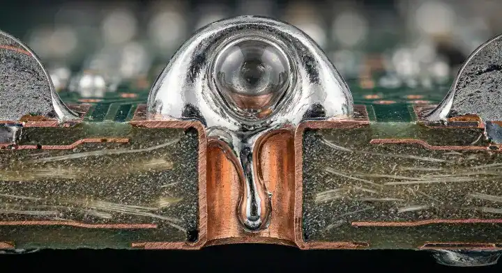
Open via-in-pad designs create massive BGA voids by acting as an open chimney that pulls in trapped air, which then rapidly expands during reflow to form bubbles far exceeding acceptable limits. Capillary action simultaneously sucks the liquid solder paste down the bare via barrel, starving the joint of metal and guaranteeing an electrically weak or completely open connection.
We frequently see questions like this one from Electronics StackExchange: “Is placing a via directly on a BGA pad bad practice? My assembly house says it’s causing voiding, but I need the routing density.”
Yes, it is the undisputed number one killer of BGA reliability. You absolutely cannot place an open via directly under a BGA ball. During the reflow oven cycle, the via hole acts exactly like a chimney, feeding expanding bottom air directly into the molten solder ball. Combined with the capillary wicking effect pulling the tin away, the joint fails completely. Industry research heavily supports this: utilizing copper-filled vias (VIPPO) slashes BGA void area by 64% to 74% compared to standard unfilled vias. If your BGA pitch is ≤0.5mm, you must specify the VIPPO process in your fab notes. If your pitch is larger and you have a restricted budget, you must at least demand an epoxy fill with a copper cap. Absolutely avoid trying to use solder mask tenting on the bottom side as a cheap alternative—the mask will easily crack under thermal expansion, re-opening the air channel. We explain these options completely in our pcb via tenting vs plugging vs filling guide.
| Treatment Method | Voiding Risk | Cost Impact | Best For | Recommendation |
|---|---|---|---|---|
| Open Via-in-Pad | Extreme (70%+) | Zero added cost | Nothing | Never use under any BGA |
| Solder Mask Tenting | High | Low | Low-density routing | Avoid for BGA pads; mask cracks |
| Epoxy Fill + Plating | Very Low | Moderate ($50-$100 NRE) | Standard BGA boards | Minimum requirement for BGA vias |
| VIPPO (Copper Fill + Cap) | Zero | High ($100-$200 NRE) | Fine-pitch (<0.5mm), HDI | Mandatory for high-reliability boards |
Choose VIPPO (copper fill and cap) for all fine-pitch HDI designs to guarantee a perfectly flat solderable surface; choose standard epoxy fill for consumer boards to save costs, but avoid open vias at all costs.
A startup client once insisted on using open via-in-pad to save a $150 NRE tooling charge. First-article inspection revealed catastrophic 45% voiding across the main processor. We halted production, redesigned the bare board fabrication files to utilize our strict VIPPO process, and the subsequent run achieved a 99.7% first-pass yield with voiding well under 8%.
Bottom line: If your BGA pitch is 0.5mm or tighter, skipping the VIPPO process to save money is actively guaranteeing a catastrophic field failure rate.
Why Does 100% Solder Paste Coverage Make Voiding Worse?
Applying 100% solder paste coverage traps flux outgassing in the exact center of the pad, commonly resulting in massive voids that push well past the bga voiding acceptable limits into the 30% to 50% area range. A proper stencil design reduces total coverage to 50–70% using a grid pattern, creating physical escape channels for the vaporized flux gases to exit before the tin solidifies.
This specific issue dominates hardware forums. Look at this common complaint from Reddit r/PrintedCircuitBoard: “We’re getting 40% voiding on a large QFN/BGA thermal pad. Tried adjusting the reflow profile but nothing helped. What stencil design should we use?”
The factory instinct is often to add more paste, but 100% coverage is fundamentally flawed. When a massive continuous layer of paste begins to reflow, the outer edges melt first. This completely seals the perimeter, trapping all the expanding flux gas violently in the center. The only way to fix this is by redesigning your stencil aperture into a “window-pane” or grid pattern. You must drop the paste coverage down to 50–70%. More importantly, you must maintain a 0.3mm to 0.5mm web width of bare pad between the grid openings. These unprinted web lines act as dedicated venting channels, allowing the gas to safely escape outward. If your large thermal pad contains thermal vias, your stencil aperture must utilize offset printing—meaning the stencil openings must actively avoid the via holes to prevent solder from wicking down. Research proves this window-pane technique drastically reduces thermal pad voiding to meet the strict IPC-A-610 Class 3 standard of <25%. For more specific alloy settings, review our avoid pcba defects the ultimate soldering paste guide.
Bottom line: Stop asking your assembly partner to add more paste to fix thermal pad voiding; ask them to intelligently segment the stencil openings instead.
What Reflow Profile Settings Reduce BGA Voiding Below 10%?
To reduce voiding below 10%, you must extend the reflow oven soak zone to 60–90 seconds at a plateau of 150–200°C. This prolonged specific stage gives the low-boiling volatile compounds inside the flux ample time to fully vaporize and escape out of the sides before the SAC305 lead-free alloy reaches its 235–250°C peak temperature.
Consider the timing: Time Above Liquidus (TAL) is equally critical. If TAL is too short, the metal freezes before the last bubbles rise to the surface; if it is too long, the flux burns off completely, causing massive oxidation and brittle intermetallic growth. A perfect TAL window sits right between 60 and 90 seconds. We also evaluate the pad design itself during the layout phase. Non-Solder Mask Defined (NSMD) pads inherently provide a tiny physical gap around the copper perimeter, which acts as a fantastic micro-trench for gas to escape, whereas SMD pads seal the edges tight.
For standard prototype runs (5–10 boards), optimizing the standard ramp-soak-spike profile drops voids cleanly to 15%; for high-volume automotive production (1,000+ boards), implementing advanced vacuum reflow technology physically sucks the gas out, slashing voiding permanently below 5%.
Bottom line: A fast ramp-up might save the factory operating time, but a prolonged, highly controlled soak zone is the only reliable thermal mechanism to push out flux gases.
Why Is 3D X-Ray the Only Reliable Way to Measure BGA Voids?

Standard 2D X-Ray inspection systematically underestimates bga voiding acceptable limits by compressing a 3D spherical joint into a flat 2D projection, frequently missing hidden gas pockets by up to 50%. Only 3D CT (Computed Tomography) slicing provides the true volumetric measurement required to definitively pass or fail a board against IPC-7095 Class 3 standards.
Here’s the technical reality: When a 2D X-Ray shoots through a PCB, it creates an effect called “X-Ray blooming,” where the dense solid tin distorts the shadow of the empty void. Furthermore, if you are building a double-sided PCBA with components mounted back-to-back, 2D X-Ray suffers from severe superimposition. The shadows of top-side capacitors blend perfectly into the bottom-side BGA balls, making accurate void calculation mathematically impossible. 3D X-Ray fixes this by taking hundreds of angled shots to reconstruct a slice-by-slice 3D model, allowing engineers to measure the exact volumetric percentage. We cover the specific machine parameters in our x-ray inspection pcb assembly guide.
| Capability | 2D X-Ray | 2.5D / Oblique X-Ray | 3D CT (Computed Tomography) | Impact on Void Measurement |
|---|---|---|---|---|
| Measurement Type | 2D Area Projection | Tilted 2D Area | True 3D Volume | 2D heavily underestimates real size. |
| Double-Sided PCBA | Fails (Overlapping shadows) | Poor | Excellent (Slices through layers) | 3D is mandatory for dense boards. |
| Micro-void Detection | Very Poor | Moderate | High Precision | 3D spots planar cracks instantly. |
| Inspection Speed | Fast (Seconds per board) | Medium | Slow (Minutes per package) | Use 3D for critical BGA checks. |
Choose basic 2D X-Ray for fast, high-volume batch checks on simple single-sided commercial boards; demand 3D CT inspection for complex double-sided PCBA or any mission-critical aerospace and medical hardware.
Bottom line: If your contract manufacturer only offers basic 2D X-Ray for complex double-sided boards, their printed voiding pass reports are essentially just optimistic guesswork.
How Do You Specify BGA Voiding Limits in Your Assembly Contract?
Specifying limits requires writing exact percentages directly into your manufacturing contract, such as demanding a maximum 15% void area per ball and capping total center thermal pad voiding at strictly 20%. You must also explicitly define that all final measurements will be verified using volumetric 3D X-Ray rather than standard top-down 2D projection.
Many engineers just write “Build to IPC-A-610 Class 2” on their drawing. That is a massive mistake. As we proved earlier, a board can technically pass Class 2 with 30% voiding and still fail in the field due to heat accumulation. You need to negotiate these terms upfront. The cost of optimizing a reflow profile or adding a window-pane stencil is effectively zero. The cost of upgrading to VIPPO fabrication is roughly $100–$200 in one-time NRE fees. Compare that to the cost of a thermal field failure: shipping the unit back, tearing down the enclosure, desoldering a massive BGA, x-raying the failure, and replacing a $50 MCU. Field failures cost 100x more than factory prevention.
Bottom line: A manufacturing contract that just says “build to IPC standards” is dangerously vague; you must hardcode exact void percentages, test equipment requirements, and stencil coverage rules into your quality agreement.
Conclusion
Letting your factory slide right up against the 25% IPC threshold is playing Russian roulette with your hardware’s thermal performance. As chip densities skyrocket, trapped gases from open via-in-pad structures, 100% stencil coverage, and rushed reflow profiles create a perfect storm for field failures.
At QueenEMS, we do not treat IPC limits as a target; we treat them as a failure. We utilize mandatory VIPPO guidelines for fine-pitch parts, optimized window-pane stencil logic, and advanced 3D X-Ray inspection on every single BGA to routinely push voiding rates safely below 10%. We catch the defects that standard 2D machines completely miss.
Don’t let invisible micro-voids ruin your next product launch. Contact us for a free DFM/DFA engineering review, and our team will analyze your bare board routing and stencil layout to guarantee a zero-defect SMT run.
Written by the QueenEMS Engineering Team
FAQ
Can IPC Class 2 boards have 35% BGA voiding? No. The absolute maximum allowable void area for an IPC Class 2 board is 30% of the individual solder ball area. Anything exceeding 30% is a defect requiring immediate rework, and you should ideally push your factory to keep rates below 15% for thermal safety.
Is vacuum reflow necessary to meet IPC-7095 limits? No, but it is the ultimate solution for high-reliability boards. A perfectly tuned standard reflow profile with a 60–90 second soak time can routinely achieve 10-15% voiding, but adding a vacuum chamber phase physically pulls trapped gas out, driving voiding definitively below 5%.
Does baking BGAs and PCBs reduce voiding? Yes, baking is highly critical. Following J-STD-033 baking standards removes absorbed ambient moisture from the substrate and component casing, preventing moisture-induced outgassing that typically forms dangerous planar microvoids directly at the solder interface.
Upload your files today · Free DFM check before production · Ship worldwide
Get your PCB prototypes in as fast as 24 hours. We handle FR4, Rogers, and Flex up to 60 layers — free prototypes for 2–4 layer boards, no minimum order.
Just upload your Gerber + BOM — we source every part, assemble, and inspect (AOI + X‑Ray) so you don't have to chase suppliers. Boards ship in as fast as 24 hours.