
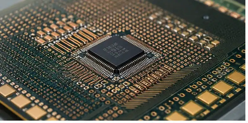
Quick Answer: Select a BT substrate for memory packaging by starting with the interconnect style, then matching CTE grade, layer count, thickness, surface finish, and warpage control to the package. Wire-bond memory packages often push ENEPIG and bondability questions, while flip-chip or DDR5-style packages require tighter low-CTE, thin-substrate, and coplanarity control.
Key takeaways
- This page covers selection mechanics; QueenEMS’ earlier memory page owns the role of BT in memory packaging.
- Wire-bond and flip-chip memory packages lead to different finish, routing, and warpage checks.
- Low-CTE BT becomes more attractive as die size grows, substrate gets thinner, or coplanarity tightens.
- The RFQ should include package map, interconnect method, finish, stack-up, and warpage target.
A memory-package buyer can know that BT is common and still struggle to select the right grade. The question is no longer why memory uses BT. It is which BT construction can survive the die size, interconnect method, reflow profile, and coplanarity limit. For the background role, see BT’s role in memory packaging. This article stays on the specification step. For a broader map of specs, applications, process limits, and sourcing questions, see the overview of BT PCB topics.
Table of Contents
- How do you select BT for memory packaging?
- Wire-bond or flip-chip drives the first choice
- What CTE grade does the die size require?
- How many layers does the package need?
- What Tg and reflow margin should be specified?
- Which surface finish fits memory substrates?
- When low-CTE BT becomes necessary
- A memory BT specification package
How do you select BT for memory packaging?
Memory BT selection starts with package architecture, not with a generic material ranking.
Commodity wire-bond packages, controller packages, DDR-style devices, and flip-chip memory carriers create different stress paths. The substrate choice must follow interconnect method, die size, substrate thickness, and assembly process.
| Decision input | Memory-package meaning | Specification action |
|---|---|---|
| Interconnect | Wire-bond, flip-chip, or package carrier path | Choose finish, pad rules, and routing density |
| CTE | Stress between die, substrate, and solder balls | Review low-CTE or ultra-low-CTE options |
| Layer count | Escape routing, planes, and signal integrity | Match layers to I/O and power map |
| Warpage | Assembly yield and coplanarity | State limit and test temperature if known |
Send the supplier the package drawing, ball map, bond or bump style, target thickness, reliability class, and expected reflow profile. Those files define the memory BT problem more clearly than a one-line material request.
Do not reuse a datasheet table as the selection answer. Datasheet values help only after the package constraints are known.
Buyer call: Name the memory package structure before choosing grade, finish, or layer count.
Wire-bond or flip-chip drives the first choice
Wire-bond and flip-chip packages pull the BT specification in different directions.
Wire-bond packages care about bondable finish, pad cleanliness, package strip handling, and stable surfaces. Flip-chip packages push bump pitch, coplanarity, low CTE, and routing precision harder.
A wire-bond RFQ should identify ENEPIG or another approved bondable finish and the bond-pad requirements. A flip-chip RFQ should state bump pitch, warpage limit, substrate thickness, and whether coreless construction is being considered.
Do not let the supplier infer the interconnect style from a Gerber alone. The same artwork can be misread without package notes.
Evidence rule: Choose finish and warpage controls from the interconnect method, then compare BT grades.
What CTE grade does the die size require?
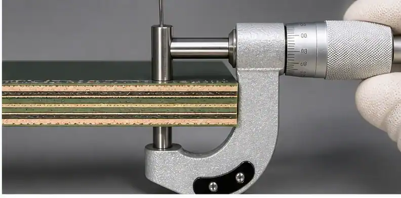
CTE grade depends on die size, substrate thickness, and assembly stress.
BT is often chosen because it can provide better CTE behavior than ordinary board laminates. Public MGC low-CTE families show several X/Y CTE options, and ultra-low variants are positioned for tighter package control.
A large die on a thin substrate should trigger a lower-CTE discussion. Smaller commodity memory packages may not need the most restrictive grade if warpage and reliability limits are still met.
CTE is not a standalone target. It must be reviewed with modulus, copper layout, strip format, and thermal history.
Engineering gate: Escalate to low-CTE BT when die stress or coplanarity becomes the yield limiter.
How many layers does the package need?
Layer count is set by I/O escape, power distribution, and signal integrity, not by a standard memory template.
A simple wire-bond memory package may use a simpler substrate, while advanced memory, controller, or SiP builds can require more layers and tighter line or space. The chosen layer count also affects thickness and warpage.
Package teams should send the pad map, plane requirements, impedance targets, and any routing keepouts. QueenEMS can then separate real layer need from over-specified layers that only add time and cost.
For broader stack-up mechanics, the companion page on BT PCB thickness and layer count is the better reference.
Quote signal: Do not add BT layers until the I/O escape and plane map prove they are needed.
What Tg and reflow margin should be specified?
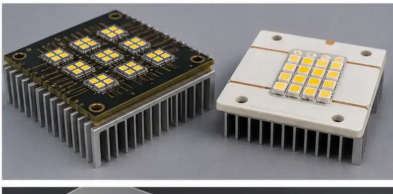
Tg and reflow margin should match the memory package’s assembly history.
Memory packages can see multiple heat events: substrate fabrication, die attach, molding, board assembly, rework, or qualification testing. A BT grade with suitable Tg and dimensional stability reduces the risk that those steps change package geometry.
The RFQ should state lead-free reflow profile, maximum temperature, number of passes when known, and any post-mold or bake requirements. A supplier can then check whether the material and finish combination is realistic.
Do not select Tg alone. A high Tg number does not remove CTE, moisture, or warpage checks.
Release check: Approve Tg only as part of the full reflow and package-stability review.
Which surface finish fits memory substrates?
Surface finish is part of the memory package design, especially when wire bonding is involved.
ENEPIG is often considered for wire-bondable surfaces because it can support gold wire bonding when properly controlled. ENIG may fit some soldering-focused builds, but the bondability question must be resolved before quotation.
Ask the supplier which finish is being quoted, the thickness range, and whether the finish has been validated for the bond or solder process. That answer belongs with pad design and package assembly notes.
Finish is not only a price item. It can decide whether the memory package can be assembled at all.
Document rule: State the required finish and bondability expectation before comparing supplier prices.

When low-CTE BT becomes necessary
Low-CTE BT becomes necessary when ordinary BT no longer controls die stress or warpage.
The trigger is usually a combination: larger die, thinner substrate, tighter coplanarity, high I/O density, or a customer reliability condition. Public low-CTE and ultra-low-CTE BT families exist because this stress problem is real in package substrates.
A useful review asks what failure is being prevented. Is the risk solder-joint fatigue, die stress, strip warpage, or assembly coplanarity? The grade should match that failure mode.
Low-CTE material can cost more and take longer. Use it where the package risk justifies it.
Design call: Specify low-CTE BT only after die size, thickness, and warpage limit make the need visible.
A memory BT specification package
A memory BT specification package should be short but complete.
Include package drawing, Gerber or ODB++ files, stack-up, target grade or equivalent rule, interconnect method, surface finish, layer count, thickness, ball or bond map, warpage limit, reflow profile, and reliability class.
That package lets QueenEMS or another supplier return a quote that separates material availability, technical deviation, and schedule risk. It also makes later supplier substitution easier to review.
For exact RFQ field wording, use QueenEMS’ what to include in a BT RFQ page.
Acceptance point: Release memory BT sourcing only after package structure, finish, CTE target, and warpage requirement are visible.
Memory selection field note: begin with the package construction, because the same word memory can describe very different substrate needs. A low-cost wire-bond memory package, a DDR5 controller package, a compact SiP, and a thin flip-chip memory device do not share one BT recipe. The interconnect method decides surface finish and pad preparation. Die size and substrate thickness drive CTE and warpage review. I/O count and plane needs decide layer count. Reflow history and moisture sensitivity decide how much thermal margin and storage control the material must support.
The surface finish choice is a common hidden blocker. A buyer may send a Gerber and ask for BT substrate quotation, while the assembler later expects a wire-bondable finish. If ENEPIG is required, it should appear in the first RFQ together with pad purpose and bond process. If ENIG is acceptable, the acceptance rule should say so. The finish decision affects price, lead time, inspection, and assembly readiness. Treating it as a late purchasing choice can invalidate a memory package quote that looked attractive at first.
Low-CTE material should be justified by package risk. Use it when the die is large, the substrate is thin, coplanarity limits are tight, or the customer requires a proven low-warpage route. Do not request the lowest possible CTE for every memory substrate, because the narrowest grade can create cost and supply limits. The better RFQ states the target package, allowed material window, warpage expectation, and whether the first lot is evaluation or production-intent. That lets QueenEMS separate a buildable sample from a qualified memory substrate path.
Project-specific checks
| Buyer check | memory package note evidence | Use before quote release |
|---|---|---|
| wire-bond path | flip-chip map | Confirms the memory package note basis before supplier comparison |
| DDR package | memory low-CTE grade | Shows which memory package note assumption needs engineering sign-off |
| memory ENEPIG finish | bond pad | Prevents a quiet memory package note substitution during pilot planning |
- Verify the wire-bond path against the memory low-CTE grade; that wire-bond path pairing protects the memory package note quote accuracy. If ball map shifts, supplier wording changes; preserve mold flow in the memory package note so the wire-bond path reviewer sees why memory low-CTE grade stayed controlled.
- Map the flip-chip map against the memory ENEPIG finish; that flip-chip map pairing protects the memory package note assembly release. If die size shifts, supplier wording changes; preserve reflow profile in the memory package note so the flip-chip map reviewer sees why memory ENEPIG finish stayed controlled.
- Record the DDR package against the bond pad; that DDR package pairing protects the memory package note customer approval. If substrate strip shifts, supplier wording changes; preserve strip warpage limit in the memory package note so the DDR package reviewer sees why bond pad stayed controlled.
- Compare the memory low-CTE grade against the ball map; that memory low-CTE grade pairing protects the memory package note supplier comparison. If mold flow shifts, supplier wording changes; preserve package outline in the memory package note so the memory low-CTE grade reviewer sees why ball map stayed controlled.
- Separate the memory ENEPIG finish against the die size; that memory ENEPIG finish pairing protects the memory package note pilot planning. If reflow profile shifts, supplier wording changes; preserve coreless option in the memory package note so the memory ENEPIG finish reviewer sees why die size stayed controlled.
- Confirm the bond pad against the substrate strip; that bond pad pairing protects the memory package note shipment acceptance. If strip warpage limit shifts, supplier wording changes; preserve memory I/O fanout in the memory package note so the bond pad reviewer sees why substrate strip stayed controlled.
- Flag the ball map against the mold flow; that ball map pairing protects the memory package note repeat-order control. If package outline shifts, supplier wording changes; preserve pilot lot in the memory package note so the ball map reviewer sees why mold flow stayed controlled.
- Freeze the die size against the reflow profile; that die size pairing protects the memory package note material continuity. If coreless option shifts, supplier wording changes; preserve wire-bond path in the memory package note so the die size reviewer sees why reflow profile stayed controlled.
- Trace the substrate strip against the strip warpage limit; that substrate strip pairing protects the memory package note quote accuracy. If memory I/O fanout shifts, supplier wording changes; preserve flip-chip map in the memory package note so the substrate strip reviewer sees why strip warpage limit stayed controlled.
- Review the mold flow against the package outline; that mold flow pairing protects the memory package note assembly release. If pilot lot shifts, supplier wording changes; preserve DDR package in the memory package note so the mold flow reviewer sees why package outline stayed controlled.
- Name the reflow profile against the coreless option; that reflow profile pairing protects the memory package note customer approval. If wire-bond path shifts, supplier wording changes; preserve memory low-CTE grade in the memory package note so the reflow profile reviewer sees why coreless option stayed controlled.
- Align the strip warpage limit against the memory I/O fanout; that strip warpage limit pairing protects the memory package note supplier comparison. If flip-chip map shifts, supplier wording changes; preserve memory ENEPIG finish in the memory package note so the strip warpage limit reviewer sees why memory I/O fanout stayed controlled.
- Screen the package outline against the pilot lot; that package outline pairing protects the memory package note pilot planning. If DDR package shifts, supplier wording changes; preserve bond pad in the memory package note so the package outline reviewer sees why pilot lot stayed controlled.
- Tie the coreless option against the wire-bond path; that coreless option pairing protects the memory package note shipment acceptance. If memory low-CTE grade shifts, supplier wording changes; preserve ball map in the memory package note so the coreless option reviewer sees why wire-bond path stayed controlled.
- Verify the memory I/O fanout against the flip-chip map; that memory I/O fanout pairing protects the memory package note repeat-order control. If memory ENEPIG finish shifts, supplier wording changes; preserve die size in the memory package note so the memory I/O fanout reviewer sees why flip-chip map stayed controlled.
- Map the pilot lot against the DDR package; that pilot lot pairing protects the memory package note material continuity. If bond pad shifts, supplier wording changes; preserve substrate strip in the memory package note so the pilot lot reviewer sees why DDR package stayed controlled.
- Record the wire-bond path against the memory low-CTE grade; that wire-bond path pairing protects the memory package note quote accuracy. If ball map shifts, supplier wording changes; preserve mold flow in the memory package note so the wire-bond path reviewer sees why memory low-CTE grade stayed controlled.
Sources
FAQ
What BT grade is used for DDR5 memory packaging?
The answer depends on package structure, die size, thickness, and warpage limits. DDR5-style or flip-chip packages often push lower-CTE and tighter coplanarity control.
Should memory BT use ENEPIG?
ENEPIG is commonly reviewed when wire bonding is required. Confirm bondability, finish thickness, and pad requirements with the assembler.
When do I need low-CTE BT?
Use low-CTE BT when large die, thin substrate, or strict coplanarity makes ordinary material too risky.
How many layers does a memory BT substrate need?
Layer count follows I/O escape, plane count, and signal needs. It should not be copied from another package without review.
Send QueenEMS your BT substrate for memory packaging package
For a memory-package substrate review, send the package outline, ball or bond map, target thickness, finish requirement, reflow condition, and warpage limit via QueenEMS package review. The resulting BT memory substrate production quotation can separate grade choice, layer count, ENEPIG or ENIG finish, and low-CTE risk.
Written by the QueenEMS Engineering Team
Upload your files today · Free DFM check before production · Ship worldwide
Get your PCB prototypes in as fast as 24 hours. We handle FR4, Rogers, and hybrid boards up to 40 layers in volume production, with advanced builds subject to engineering review — free prototypes for 2–4 layer FR-4 boards, no minimum order.
Just upload your Gerber + BOM — we source every part, assemble, and inspect (AOI + X‑Ray) so you don't have to chase suppliers. Boards ship in as fast as 24 hours.