
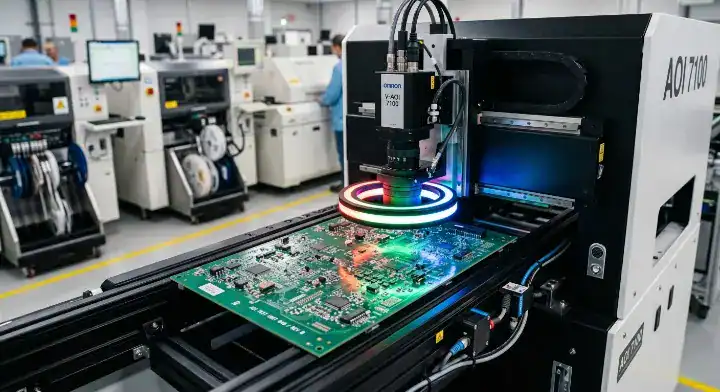
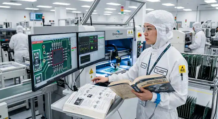
Quick Answer: The AOI full form means Automated Optical Inspection, a vision-based diagnostic system that uses high-resolution cameras and multi-angle lighting to detect PCB assembly defects. It scans printed circuit boards at speeds of up to 150 square centimeters per second, capturing 95% to 98% of visible surface anomalies like solder bridges and missing components. Key takeaways:
- AI-powered optical scanners reduce false positive rates by 30% to 40%.
- 3D inspection improves volume measurement accuracy by 15% over standard 2D systems.
- Optical systems cannot detect hidden BGA joints, which means X-ray integration is mandatory.
- High-volume SMT lines typically recoup their $50,000 to $150,000 optical equipment investment within 8 to 12 months.
Manual visual checks miss hidden solder defects on high-density boards, resulting in expensive rework cycles and rejected shipments. By integrating an AOI full form methodology into your surface mount technology (SMT) line, you systematically eliminate human error. This guide breaks down how vision-based diagnostics operate, the exact defects they catch, and when to pair them with X-ray screening to achieve a 99.7% first-pass yield.
Table of Contents
- 1. What Does the AOI Full Form Mean in PCBA?
- 2. How Does the AOI Full Form System Work?
- 3. Where Is AOI Full Form Used in Production?
- 4. What Defects Can AOI Full Form Detect?
- 5. Why Do Lights Matter in AOI Full Form?
- 6. 2D vs 3D AOI Full Form: Which to Choose?
- 7. AOI Full Form vs X-Ray: When to Use Which?
- 8. How Do IPC Standards Affect AOI Full Form?
- 9. What Are the Costs of AOI Full Form Tools?
- 10. How to Cut False Calls in AOI Full Form?
1. What Does the AOI Full Form Mean in PCBA?
The AOI full form stands for Automated Optical Inspection, a machine-vision system that actively scans printed circuit boards for catastrophic manufacturing errors. This equipment captures highly detailed images of every component and solder joint, maintaining a positional verification accuracy of ±0.025mm.
Defining the Optical Inspection Process
Machine vision inspection replaces subjective human evaluations with mathematical precision. You upload a known-good CAD design into the software, which means the machine has a flawless baseline for comparison. The system then analyzes every manufactured board against this digital twin. Here are the facts:
- Operating speed hits 0.5 seconds per frame.
- Detection resolution scales down to 10 micrometers.
- The system evaluates both geometric placement and solder volume.
Why Human Verification Falls Short
Human operators suffer from eye fatigue after just 20 minutes of inspecting high-density PCBA boards. A standard 6-layer board contains over 2,000 individual solder joints, making manual verification mathematically unviable for batch production.
Bottom line: Transition entirely to automated optical scanning for any production run exceeding 50 units to eliminate fatigue-induced inspection errors.
| Inspection Method | Speed (Units/Hour) | Defect Capture Rate | Fatigue Drop-off |
|---|---|---|---|
| Manual Operator | 15-20 | 65-75% | High |
| Automated Optical | 250-400 | 95-98% | Zero |
Deploying machine vision consistently outperforms human operators in both throughput volume and sustained defect capture accuracy.
2. How Does the AOI Full Form System Work?
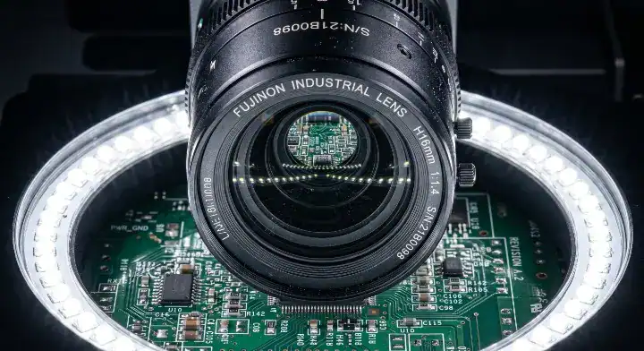
Understanding the AOI full form mechanics reveals a synchronized operation of LED lighting arrays, industrial camera lenses, and proprietary image processing software. These units project multi-colored light patterns onto the board surface, capturing the structural reflections to identify variations as small as 5 microns.
The Role of Industrial Cameras
High-resolution industrial cameras form the mechanical core of any visual diagnostic unit. Top-tier machines utilize 12-megapixel to 25-megapixel sensors mounted on high-speed gantry systems. Look at the technical specifications:
- Top-down lenses capture lateral component shifts.
- Side-angled cameras verify lifted leads on QFP packages.
- Telecentric lenses eliminate perspective distortion on tall capacitors.
Pattern Matching Algorithms
The software engine powers the actual decision-making process during scanning. Pattern matching is an algorithmic method where the system calculates the pixel-by-pixel correlation between the captured image and the reference library.
Bottom line: Verify that your inspection equipment utilizes statistical pattern matching rather than basic pixel counting to prevent acceptable variations from triggering false alarms.
| Component Requirement | Function | Target Metric |
|---|---|---|
| Main Camera Sensor | Image capture | 12MP – 25MP |
| Angled Side Lenses | Lead verification | 4 to 8 units |
| Processing Software | Image calculation | <10ms per frame |
Higher megapixel counts directly correlate with the machine’s ability to identify micro-defects on tightly packed 01005 passive components.
3. Where Is AOI Full Form Used in Production?
The AOI full form diagnostic approach deploys at three distinct manufacturing chokepoints: immediately after solder paste printing, after component placement, and following the final reflow oven. Catching a misaligned resistor before it enters the reflow oven prevents hard-soldered defects, resulting in a 10x reduction in rework expenses.
Pre-Reflow vs Post-Reflow
A client previously skipped post-paste inspection, leading to 12% board failure rates due to hidden solder bridging. We integrated 3D SPI (Solder Paste Inspection) and pre-reflow optical checks directly into their SMT assembly line. This immediate intervention dropped their end-of-line rework by 45% and locked their first-pass yield at a stable 99.7%. Consider these strategic placement locations:
- Post-paste checks volume and alignment.
- Pre-reflow catches missing parts before baking.
- Post-reflow verifies final solder fillet shapes.
Solder Paste Inspection Integration
Solder Paste Inspection (SPI) serves as the first line of defense in the surface mount process. Because 70% of all soldering failures originate from poor paste deposition, analyzing paste volume and height instantly isolates printer issues.
Bottom line: Always mandate SPI checks directly after stencil printing to catch insufficient paste volumes before expensive integrated circuits are placed.
| Assembly Stage | Inspection Focus | Rework Cost Impact |
|---|---|---|
| Post-Paste (SPI) | Solder volume, alignment | Lowest ($) |
| Pre-Reflow | Component presence, skew | Medium ($$) |
| Post-Reflow | Fillet shape, tombstones | Highest ($$$) |
Catching anomalies before the reflow oven significantly reduces the thermal stress associated with desoldering and replacing hard-fixed components.
4. What Defects Can AOI Full Form Detect?
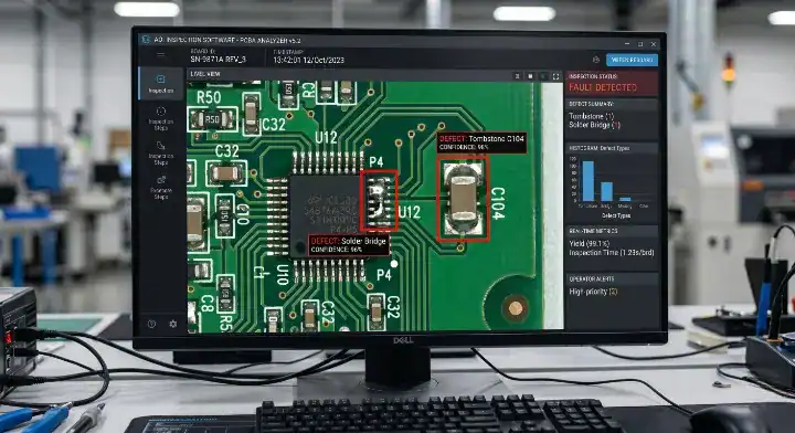
The AOI full form equipment actively identifies missing components, catastrophic solder bridges, passive billboarding, and severe polarity mismatch errors. High-end optical platforms achieve a 98% defect capture rate for visible surface anomalies on microscopic 0201 packages.
Typical Surface Mount Anomalies
Tombstoning is a thermal defect where a passive component stands vertically on one end during the reflow process. It typically accounts for 15% to 20% of all surface mount failures on tiny 0402 packages. Review this defect coverage list:
- Solder bridges between fine-pitch IC pins.
- Insufficient solder causing weak mechanical bonds.
- Reversed diode polarity leading to circuit failure.
Solving the False Positive Problem
(1) Question: “AOI keeps flagging false positives on acceptable solder joints, wasting operator time to manually verify each board. How to reduce false call rate?” (Source: EEVBlog Forum) AI-based optical scanners reduce false positives by 30% to 40% by learning from historical operator verifications. Proper multi-angle lighting configuration physically reduces shadow-related false calls. Furthermore, regular machine calibration every 1 to 3 months is mandatory to keep the baseline accuracy strict.
Bottom line: Implement AI-assisted review software on your factory floor to filter out acceptable physical variations and keep your false positive rate below 2%.
| Defect Type | Description | Optical Detection Rate |
|---|---|---|
| Tombstoning | Component stands vertically | 99% |
| Solder Bridges | Shorts between adjacent pins | 98% |
| Missing Parts | Empty copper pads | 100% |
Optical systems excel at finding geometric and presence-based errors but depend entirely on clear line-of-sight to the copper pad.
5. Why Do Lights Matter in AOI Full Form?
Lighting configurations in an AOI full form setup determine the physical contrast and exact defect visibility for the camera sensors. Red, green, and blue (RGB) light emitting diodes project beams from varying angles, mapping three-dimensional solder shapes into readable two-dimensional color gradients.
Multi-Angle LED Topography
The software misinterprets flat reflections, which means a single overhead light source cannot accurately verify sloped solder joints. By utilizing a tiered ring light setup, steep solder fillets reflect red light, while flat surfaces reflect blue light back to the lens. Here is how lighting angles perform:
- High-angle lighting illuminates flat pad surfaces.
- Mid-angle lighting catches component body edges.
- Low-angle lighting highlights steep solder meniscus curves.
Overcoming Shadow Limitations
Tall electrolytic capacitors frequently cast dark shadows over adjacent microscopic resistors. Coaxial lighting projects light perfectly straight down through the lens axis, eliminating these blind spots entirely.
Bottom line: Demand a programmable RGB multi-angle lighting dome on your inspection equipment to guarantee visibility across mixed-height component topographies.
| Light Angle | Reflected Surface | Primary Function |
|---|---|---|
| High (Top-Down) | Flat component bodies | Reads laser-etched part numbers |
| Medium (45 deg) | Slight slopes | Checks component alignment |
| Low (Horizontal) | Steep solder fillets | Verifies joint volume and shape |
Strategic color blending allows the software to calculate exact angles and slopes based on which color wavelength bounces back to the primary sensor.
6. 2D vs 3D AOI Full Form: Which to Choose?
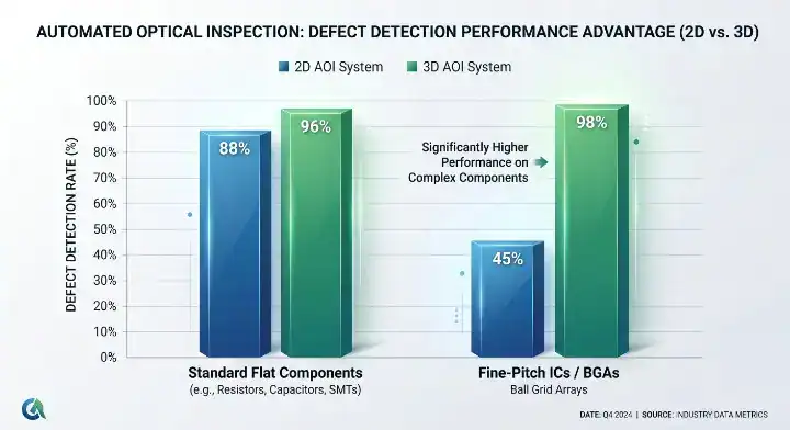
Moving from 2D to a 3D AOI full form infrastructure adds precise height and volume measurements to your quality control protocol. A 3D scanner utilizes moiré fringe projection to measure solder fillet heights down to a 1-micron resolution, catching lifted pins that flat 2D cameras completely miss.
When 2D Inspection Is Sufficient
An EV startup initially relied on 2D optical checks, missing lifted leads on heavy copper pads because they lacked Z-axis height data. We migrated their production to a 3D optical line utilizing multi-fringe projection arrays. Their field failure rate immediately dropped to zero, eliminating $12,000 monthly in warranty replacement claims. Consider these parameters for 2D setups:
- Works perfectly for flat, standard passive resistors.
- Processes boards 20% faster than 3D algorithms.
- Requires less data storage for image logging.
Justifying the 3D AOI Upgrade
(2) Question: “Is 3D AOI worth the extra investment over 2D for a mid-volume SMT line? What’s the actual detection rate improvement?” (Source: EEVBlog Forum) Upgrading to 3D systems actively improves your defect detection rates by 10% to 15% specifically for solder joint height and volume anomalies. Basic 2D scanners remain adequate for simple legacy boards utilizing standard components. However, 3D profiling is fundamentally essential for fine-pitch QFN and 01005 packages to prevent latent field failures.
Bottom line: Purchase a 3D inspection unit if your product designs include any fine-pitch ICs or leadless packages where solder volume dictates mechanical reliability.
| System Type | Height Measurement | False Call Rate | Best Application |
|---|---|---|---|
| 2D Optical | None (Flat pixel data) | 5 – 8% | Simple boards, basic passives |
| 3D Optical | Yes (1-micron accuracy) | < 2% | QFNs, high-density aerospace |
The integration of Z-axis data structurally eliminates the false positives caused by varying board colors and silkscreen misalignments.
7. AOI Full Form vs X-Ray: When to Use Which?
The AOI full form diagnostic path handles external visual surface checks, while Automated X-Ray Inspection (AXI) safely penetrates solid physical packages. Optical scanners verify a surface component’s presence in 0.5 seconds, whereas X-ray machines require up to 2 minutes to calculate the density of hidden solder balls.
Blind Spots of Optical Methods
Because optical lenses cannot see through solid plastic or silicon, any joint located underneath a component body remains completely uninspected. This limitation leaves modern high-density designs vulnerable to hidden voiding. Here are the facts regarding testing limitations:
- Optical cameras cannot see BGA solder balls.
- Optical cameras cannot evaluate barrel fill in through-holes.
- Neither method can verify active electrical logic.
Combining X-Ray and ICT Strategies
(3) Question: “Our CM only does AOI. Is that enough or do we need X-ray too for BGA boards?” (Source: Reddit r/PrintedCircuitBoard) Optical scanners absolutely cannot inspect hidden joints under BGA or QFN packages, which means X-ray screening is mandatory for these specific boards. Combining optical checks with X-ray covers 95%+ of all physical manufacturing defects. In-Circuit Testing (ICT) then adds the electrical continuity verification that vision technologies cannot execute.
Bottom line: You must mandate X-ray inspection alongside optical scanning for any circuit board containing Ball Grid Arrays or Bottom Terminated Components.
| Inspection Type | Target Defect Area | Speed | Penetration |
|---|---|---|---|
| Automated Optical | Surface components | Very Fast | Zero |
| Automated X-Ray | Hidden BGA voids | Slow | High |
| In-Circuit Test (ICT) | Electrical shorts/opens | Fast | N/A (Electrical) |
Combining visual, internal, and electrical testing protocols creates an impenetrable quality firewall for medical and automotive electronics.
8. How Do IPC Standards Affect AOI Full Form?
IPC-A-610 guidelines define the strict pass and fail thresholds programmed directly into your AOI full form software database. Class 3 manufacturing requirements demand thicker solder fillets and tighter component alignment, pushing your optical inspection hardware to its absolute highest sensitivity settings.
Class 2 vs Class 3 Variations
A Class 2 consumer electronic product allows for a slight 50% overhang on a passive component pad. Conversely, Class 3 aerospace standards strictly limit that overhang to 25%, requiring the machine’s programming tolerances to adapt accordingly. Observe how standards alter programming:
- Heel fillet height thresholds increase for Class 3.
- Minimum solder volume parameters are raised significantly.
- Acceptable skew angles become much narrower.
Programming Verification Tolerances
Engineers must manually dial in the inspection algorithms to match the specific IPC class designated on the fabrication drawing. Setting Class 3 parameters on a Class 2 commercial board triggers a massive wave of false failures, halting production needlessly.
Bottom line: Synchronize your machine’s software threshold parameters explicitly with your target IPC class to balance perfect reliability against production throughput.
| IPC Classification | End-Use Application | Tolerance Strictness | False Call Risk |
|---|---|---|---|
| Class 1 | Cheap toys | Very Loose | Low |
| Class 2 | Standard computers | Moderate | Medium |
| Class 3 | Aerospace / Medical | Extremely Strict | High |
Tighter IPC requirements mandate higher resolution cameras and significantly slower scanning speeds to verify minute solder meniscus details.
9. What Are the Costs of AOI Full Form Tools?
Deploying an AOI full form strategy requires a tangible capital investment ranging from $30,000 for basic 2D benchtop units to well over $150,000 for inline 3D automated machines. A high-volume facility assembling 5,000 complex boards weekly typically recoups this initial equipment cost within 8 to 12 months.
Capital Investment Ranges
A medical device client refused to pay automated optical programming fees for a small 50-piece prototype run, resulting in slow manual checks. We utilized our offline CAD-based automated programming to absorb the setup time at zero extra cost. This decision caught three critical polarity errors instantly, saving their entire $4,500 prototype batch from destruction. Review the typical financial metrics:
- Benchtop 2D systems range from $20,000 to $40,000.
- Inline 3D setups range from $80,000 to $150,000.
- Annual software licensing and maintenance add 10%.
Calculating ROI for Mid-Volume Runs
The Return on Investment (ROI) equation relies on calculating the money saved from reduced rework labor and eliminated scrap boards. If a factory saves 20 hours of manual rework weekly at $50 per hour, a $100,000 inspection machine pays for itself in just two years.
Bottom line: Do not evaluate optical inspection equipment purely as a sunk cost; calculate the exact financial savings generated by eliminating field warranty replacements.
| Equipment Setup | Estimated Cost | Setup Time per Board | Break-Even Volume |
|---|---|---|---|
| Benchtop 2D | $30,000 | 2 – 3 hours | Low / Prototype |
| Inline 3D Platform | $120,000 | 1 – 2 hours (CAD) | High / Continuous |
High-end inline systems actually feature faster programming times because they automatically import and map CAD coordinates directly to the sensor library.
10. How to Cut False Calls in AOI Full Form?
Optimizing an AOI full form architecture involves upgrading from rigid template matching to flexible, pattern-based statistical modeling. AI-driven vision software actively analyzes 10,000 historical solder joints, dynamically adjusting its own tolerances and cutting the operator’s manual verification time in half.
AI and Machine Learning Integration
Legacy software triggers an alarm the moment a solder joint deviates 1 pixel from the golden board photograph. Modern machine learning algorithms, however, understand acceptable variances in solder flow, which means they safely ignore harmless cosmetic differences. Look at the optimization techniques:
- Switch from image-based to CAD-based programming.
- Train the AI model using both good and bad samples.
- Implement a central server to share learned data across machines.
Golden Board vs CAD-Based Programming
Using a single “golden board” to program your system creates baseline errors because even a perfect physical board contains microscopic anomalies. CAD-based programming pulls flawless geometric data directly from your ODB++ files, resulting in a mathematically perfect reference model.
Bottom line: Transition your factory programming protocol from physical golden boards to direct CAD data imports to eliminate baseline errors and drastically speed up NPI setups.
| Programming Method | Data Source | Setup Speed | False Call Rate |
|---|---|---|---|
| Golden Board | Physical PCB photo | Slow (Manual teaching) | Moderate |
| CAD-Based | ODB++ / Gerber data | Very Fast | Very Low |
Pulling inspection parameters directly from engineering files guarantees that the machine evaluates the board exactly as the original hardware designer intended.
When your boards fail in the field due to a bridged pin that a tired human operator missed, your brand reputation takes the actual damage. Automated optical inspection secures your product reliability, providing the quantitative data needed to scale up your manufacturing without fear. If you need flawless, machine-verified printed circuit boards for your next NPI run, contact us today to utilize our fully integrated 3D inspection assembly lines.
FAQ
Can I rely entirely on optical inspection for my PCBA testing? No, you cannot use optical scanning as your only testing method. Optical cameras only detect visual surface anomalies; you must integrate X-ray for hidden BGA joints and ICT for active electrical logic verification. Contact our engineering team to develop a custom multi-stage testing protocol.
What’s the best way to reduce the false positive rate on my machine? Upgrading to AI-based pattern matching software is the absolute best method. This reduces false flags by up to 40% because the algorithm learns to ignore acceptable cosmetic solder variations. Reach out to our facility to see our low-false-call AI systems in action.
How do I know if I need a 3D scanner instead of a 2D one? Yes, you definitively need 3D capabilities if your design includes fine-pitch components like QFNs or BGAs. 3D systems measure exact solder volume and height, which is mandatory for securing leadless component reliability. Submit your Gerber files to us for a free DFM review to determine your exact inspection requirements.
Will optical inspection slow down my overall production line? No, modern inline optical machines operate flawlessly at line speed. They scan complex boards at up to 150 square centimeters per second, easily keeping pace with high-speed surface mount placement machines. Partner with us to experience zero-bottleneck, high-volume manufacturing.
Can optical machines detect incorrect component values? No, optical cameras cannot read the electrical resistance or capacitance value inside a blank passive component. They can read laser-etched part numbers on ICs, but you must use In-Circuit Testing (ICT) to verify blank passive values. Let our assembly experts design a comprehensive DFT (Design for Test) strategy for your next project.
Upload your files today · Free DFM check before production · Ship worldwide
Get your PCB prototypes in as fast as 24 hours. We handle FR4, Rogers, and Flex up to 60 layers — free prototypes for 2–4 layer boards, no minimum order.
Just upload your Gerber + BOM — we source every part, assemble, and inspect (AOI + X‑Ray) so you don't have to chase suppliers. Boards ship in as fast as 24 hours.