
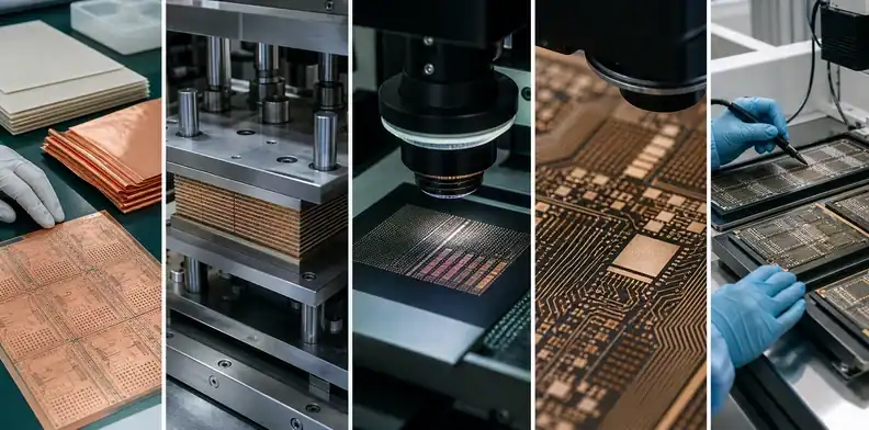
Quick Answer: The BT PCB manufacturing process starts with BT laminate or prepreg selection, then moves through inner-layer imaging, lamination, drilling or laser microvias, copper patterning, solder mask, surface finish, profiling, electrical test, and inspection. The process resembles advanced PCB fabrication, but BT adds tighter control around fragility, microvia quality, warpage, and package-level acceptance.
Key takeaways
- BT manufacturing is not a single process; subtractive etching, SAP, and mSAP routes may all appear depending on line width and package class.
- Lamination, finish, and warpage are deep topics of their own, so this page gives the full flow and links to the detailed pages.
- BT is generally more process-sensitive than standard FR-4 because package substrates are thinner, tighter, and less forgiving.
- A quote should identify material family, line/space, microvia plan, finish, thickness, inspection, and whether the build is board-like or package-like.
Many buyers picture BT as just another PCB material. That is only partly true. A BT build may pass through familiar fabrication steps, yet the controls are closer to package-substrate manufacturing when the design uses fine pitch, thin cores, microvias, or strict coplanarity. This overview explains the full sequence without turning lamination, finish, or warpage into their own textbooks. For the surrounding decisions across material data, package needs, process limits, and purchasing evidence, use the full BT PCB reference.
| Process stage | BT-specific control | Buyer question |
|---|---|---|
| Material preparation | Grade and storage | Which BT family is quoted? |
| Laser microvias | Capture and plating | What evidence proves the via? |
| Final finish | Soldering or bonding | Which attach method is supported? |
| Route type | When it appears | Quote risk |
|---|---|---|
| Subtractive copper | Moderate geometry | Feature width and copper thickness |
| mSAP or SAP | Fine package routing | Supplier class and yield |
| Coreless build | Ultra-thin carrier | Handling and warpage |
Table of Contents
- How is a BT PCB manufactured?
- Material preparation: BT CCL and prepreg
- Imaging, drilling, and laser microvias
- Subtractive vs SAP and mSAP patterning
- Where lamination fits in
- Surface finish, profiling, and final test
- How BT processing differs from FR-4
- What to send when ordering BT fabrication
How is a BT PCB manufactured?
A BT PCB is manufactured by selecting the BT material set, forming copper layers, laminating the stack, creating holes or microvias, plating and patterning copper, applying mask or dielectric where required, finishing exposed pads, and verifying the finished substrate. The exact flow depends on whether the design is a board-like BT PCB, an IC package substrate, an SLP-style build, or a coreless package carrier. Process signal: Ask for the route, not only the resin name.
Material preparation: BT CCL and prepreg
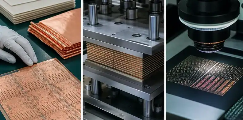
The process starts with copper-clad laminate, prepreg, or build-up material. Low-CTE BT material families may offer thin CCL and prepreg options, and MGC lists BT lines for IC plastic packages with low CTE, low shrinkage, and coreless suitability. The supplier chooses a material set based on thickness, layer count, CTE target, drilling needs, and availability. Material rule: The first manufacturing step is a controlled material choice, not the first copper image.
Imaging, drilling, and laser microvias
After material selection, the fabricator images copper layers and creates mechanical or laser-formed interconnections. BT’s glass reinforcement and resin behavior make drilling and laser parameters important, especially for small vias and thin substrates. Package-style builds may require microvias in the 25-50 micrometer class, but practical capability depends on the supplier and stack. Via check: A BT microvia quote should include diameter, stack position, plating plan, and inspection evidence.
Subtractive vs SAP and mSAP patterning
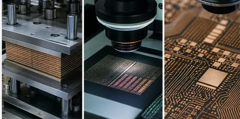
Copper patterning may use subtractive etching, SAP, or mSAP depending on feature size and substrate class. Subtractive processing removes unwanted copper from a foil. SAP and mSAP build finer copper patterns from a seed layer and plating sequence, which can support tighter line/space than a conventional subtractive route. For background, see PCB etching and fabrication. Routing rule: The process route should be selected from the finished feature target, not from a generic preference for mSAP.
Where lamination fits in
Lamination fits early and may repeat during sequential build-up. It bonds cores, prepregs, and copper structures into the stack while controlling resin flow, cure, dimensional movement, and void risk. This overview does not repeat the dedicated BT lamination and layup article. Lamination call: In a BT process review, lamination is the stage where thickness, registration, and flatness start to become real.
Surface finish, profiling, and final test
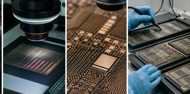
After copper patterning and mask or dielectric work, the substrate receives its surface finish. ENIG, ENEPIG, OSP, or another finish may be selected according to soldering, wire bonding, storage, and cost. Final profiling and testing then confirm outline, dimensions, electrical continuity, and inspection records. Use BT surface finish options and controlling BT warpage when those areas drive release. Final-step rule: BT fabrication is not complete until finish and outgoing evidence match the assembly method.
How BT processing differs from FR-4
BT processing differs from FR-4 because the build is often thinner, more dimensionally sensitive, and closer to package-substrate tolerances. Standard FR-4 may tolerate wider features, ordinary drilling, and less severe coplanarity control. BT substrates often require closer attention to material shrinkage, laser microvias, copper balance, finish, and reflow flatness. Supplier signal: A serious BT fabricator explains the control points; it does not treat the job like a normal FR-4 board with a different laminate.
What to send when ordering BT fabrication
Send Gerber or ODB++ files, drill data, stack-up, material target, finished thickness, line/space, via structure, finish, controlled dimensions, impedance or RF notes, warpage requirement, inspection needs, quantity stages, and shipment country. Keep the fabrication file set under a controlled revision so CAM comments, process limits, and accepted alternates are traceable before release.
Extra buyer notes for process visibility
The BT process flow should be visible enough for a buyer to understand the risk without forcing the factory to disclose proprietary recipes. Ask for the named process route, not the detailed chemical settings. For example, the supplier can state whether the pattern is subtractive, SAP, or mSAP; whether the microvias are laser formed; whether the stack uses sequential lamination; and whether finish evidence will be supplied.
Panel planning also affects manufacturing. A package substrate with small units may require tight panel registration, careful carrier handling, and singulation planning. If the outline, slots, fiducials, or array notes are unclear, the supplier may quote a layout that is difficult to assemble or inspect. Buyers should include array requirements and any downstream pick-and-place constraints when the substrate goes into module assembly.
Inspection belongs at several stages, not only at shipment. Inner-layer AOI, via inspection, plating checks, dimensional measurement, electrical test, and finish thickness measurement may all matter depending on the design. A quote does not need every report by default, but the buyer should know which evidence is included and which evidence adds cost or lead time.
Process capability should be judged against repeat production, not a single heroic sample. If the first article uses a marginal microvia, very tight line/space, or fragile coreless stack, ask what changes when the order moves from prototype to pilot. That answer tells engineering whether the design is ready or still using prototype permission.
The material preparation stage should include storage and handling assumptions. Thin BT prepreg and laminate can be more sensitive to moisture and handling damage than a buyer expects from ordinary board stock. Ask whether the supplier controls bake, storage, and floor exposure before lamination or laser processing.
After imaging, registration becomes a package-level concern. A small shift that would be acceptable on a larger FR-4 board may move a bond finger, solder land, or microvia capture pad enough to hurt yield. The supplier should state whether the layer registration target is routine or requires tighter process control.
Plating evidence is important when microvias or fine pads are involved. The buyer may need cross-section, plating thickness, via fill, or continuity evidence depending on the package. A basic electrical test can confirm connectivity but may not prove that a high-reliability via has enough copper or fill quality.
Solder mask or dielectric definition should not be assumed. Some package substrates may use solder mask differently from ordinary PCBs, and some exposed pad areas require tighter clearance or cleaner definition. If the assembly process uses wire bonding, flip chip, or small solder balls, the mask opening and finish area should be reviewed before fabrication.
Final inspection should include the evidence that protects the next process. For an assembled module, that may be coplanarity, finish thickness, surface cleanliness, or dimensional data. For a bare substrate shipped to another assembler, packaging and labeling also matter because the receiving team must connect the lot to the released files.
How buyers should read a BT process quote
A BT process quote should show which steps are standard and which steps are special. Standard may include material cutting, imaging, lamination, drilling, plating, solder mask, finish, electrical test, and profile. Special may include coreless handling, sequential build-up, mSAP, fine microvias, ENEPIG for bonding, or extra warpage reporting. The distinction helps the buyer understand why two quotes differ.
Material stage questions should focus on grade and availability. Ask whether the supplier is quoting the requested BT grade, an approved equivalent, or a material family that still needs engineering review. Material lead time can drive schedule, and a quiet substitution can change CTE, moisture, Dk, Df, or warpage behavior.
Drilling and laser processing should be tied to the real via plan. A quote should not simply say microvia supported. It should say whether the via diameter, capture pad, stack position, and plating requirement are within routine capability. When a microvia is near the supplier’s limit, a cross-section plan or first-article evidence may be worth the cost.
Patterning questions should focus on feature target and yield. If mSAP is quoted, ask what line/space and copper thickness the route supports in production. If subtractive processing is quoted, ask whether the copper thickness and fine lines are compatible. The buyer does not need the chemistry recipe; the buyer needs a reliable boundary.
Final shipment evidence should match the receiving team. A bare substrate going to an assembler may need a different document set than an assembled module. Labeling, revision, material identity, finish, and inspection data should travel with the lot so the next team does not have to reconstruct the manufacturing route from email.
Process questions that separate real BT suppliers
Ask how the supplier classifies the build. Board-like BT, package substrate, SLP-style build, and coreless carrier are different manufacturing conversations. A supplier that can place the design in the right class is more likely to quote the correct controls.
Ask which step drives lead time. The answer might be material availability, laser drilling, mSAP, ENEPIG, sequential lamination, inspection, or engineering review. Knowing the driver helps the buyer decide whether to change design, accept schedule, or request an alternate process.
Ask which evidence is included before shipment. For some BT builds, electrical test and visual inspection may be enough. For package substrates, the buyer may need finish thickness, dimensional data, cross-section, or warpage evidence. The evidence list should match the package risk.
Ask what changes if the order scales. A supplier may hand-hold a prototype but require a design relaxation for production. That is not a failure; it is useful information. The buyer should capture it before the first prototype becomes the production baseline.
What should appear in the manufacturing handoff?
The manufacturing handoff should include the released file revision, stack-up, material family, process route, finish, inspection evidence, and any open engineering assumptions. It should also state whether the substrate is intended for prototype learning, pilot production, or repeat production. Those categories often use different evidence levels.
For a package-like BT build, the handoff should travel to the assembler. A fabricator may build the substrate correctly, but assembly can still fail if the assembler does not know the finish, flatness, pad function, or storage condition. The buyer should connect fabrication evidence to assembly intake.
When the supplier asks a DFM question, capture the answer in the drawing or release note rather than leaving it buried in email. BT process decisions often affect repeatability, so the next lot should not depend on memory.
For small-batch overseas orders, ask whether the supplier will preserve the same process route for repeats. A prototype built with extra manual attention can hide process risk. The repeat quote should state whether material, finish, via structure, and inspection stay the same.
If the buyer needs assembly after fabrication, the process quote should also state whether substrates ship in panels, arrays, trays, or singulated units. That packaging choice affects handling, inspection, and pick-and-place setup. A technically good substrate can still create delay when the physical delivery format does not match the assembler’s intake process.
Upload the Gerber or ODB++ package, drill data, stack-up, material target, fine-feature limits, finish, inspection needs, and delivery format from the QueenEMS contact page. QueenEMS can compare the BT process quote path with the intended build before CAM questions slow the release.
FAQ
How is BT PCB made?
BT PCB is made through material preparation, imaging, lamination, drilling or laser microvias, plating and patterning, finish, profiling, test, and inspection.
Is BT harder to process than FR-4?
Usually yes for package-style builds. Thin material, fine pitch, microvias, and warpage control make the process more sensitive.
What is mSAP in BT manufacturing?
mSAP is a semi-additive copper process used when the required line/space is finer than a conventional subtractive route can support with good yield.
Does every BT design need ENEPIG?
No. ENEPIG is common for wire bonding or mixed assembly needs. ENIG or other finishes may fit solder-only builds.
Sources
- Mitsubishi Gas Chemical, Low-CTE BT resin laminate lineup
- Global Electronics Association, IPC-6921 organic IC substrate standard
Written by the QueenEMS Engineering Team
Upload your files today · Free DFM check before production · Ship worldwide
Get your PCB prototypes in as fast as 24 hours. We handle FR4, Rogers, and Flex up to 60 layers — free prototypes for 2–4 layer boards, no minimum order.
Just upload your Gerber + BOM — we source every part, assemble, and inspect (AOI + X‑Ray) so you don't have to chase suppliers. Boards ship in as fast as 24 hours.