
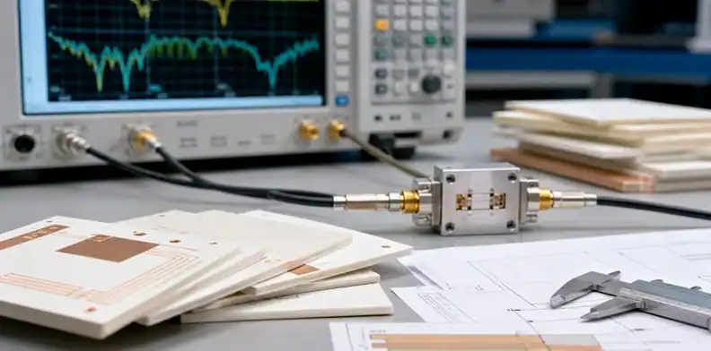
Quick Answer: Ceramic PCB dielectric constant tells RF engineers how strongly the substrate affects impedance, wavelength, coupling, and resonant behavior, while dielectric loss affects insertion loss and heating at frequency. Alumina, AlN, LTCC, and thin-film ceramic routes can all be useful, but their Dk and Df values must be tied to frequency, test method, material grade, thickness, conductor process, and supplier stackup. A quote is not RF-ready until the supplier states the dielectric data basis and what may change during fabrication.
Use the ceramic selection map if material names and conductor processes are still mixed together in the specification. Establish that distinction before requesting dielectric data.
- Dk affects impedance and physical size; Df affects loss and RF margin.
- Ceramic material data must be tied to frequency and construction before it enters a field solver.
- RF buyers should ask for stackup, material grade, conductor route, finish, tolerance, and test evidence.
RF buyers often ask for a ceramic PCB because the design is small, hot, high frequency, or package-like. The next question is usually about dielectric constant. A supplier may answer with a single number, but RF performance depends on how that number was measured and how the final construction uses it.
Choose the module architecture with the RF and microwave substrate selection guide, then connect its dielectric assumptions to the ceramic RF layout and DFM review. The dielectric record should identify which supplier value the model uses and why.
Table of Contents
- What does ceramic PCB dielectric constant control?
- How is dielectric loss different from Dk?
- Why must Dk and Df be tied to frequency and method?
- Which ceramic routes need the strictest dielectric review?
- What should RF engineers send before the quote?
- How should suppliers document dielectric assumptions?
- How should buyers compare ceramic and RF laminate options?
What does ceramic PCB dielectric constant control?
Ceramic PCB dielectric constant controls how electromagnetic fields behave in and around the substrate. In practical RF terms, Dk affects trace impedance, wavelength, phase, coupling, resonant size, antenna tuning, filter behavior, and the geometry needed to hit a target.
A higher Dk can make RF structures physically smaller, which is useful in compact modules and ceramic packages. The trade-off is that geometry and tolerance become more sensitive. A small change in line width, ceramic thickness, fired dimension, copper thickness, or nearby ground feature can move the electrical result.
For purchasing, Dk should never be treated as a loose catalog value. The RF engineer needs to know the material grade, thickness, frequency, test method, and whether the supplier’s value is a typical datasheet value or a construction-specific design value. Without that distinction, the same Gerber can be quoted as several different RF products.
Put Dk into the RFQ as a controlled design input, not as a generic material property.
How is dielectric loss different from Dk?
Dielectric loss is different from Dk because it describes how much RF energy is dissipated in the substrate, usually through dissipation factor or loss tangent. Dk mainly shapes impedance and wavelength; Df contributes to insertion loss, heating, gain reduction, filter loss, and link budget pressure.
At low frequencies or short RF paths, dielectric loss may not dominate the decision. At microwave and mmWave frequencies, or across longer paths, loss can become the reason to change material or construction. That is why RF laminate suppliers and ceramic suppliers both publish dielectric data, but those values are useful only when the test frequency and method are understood.
For ceramic PCB, the conductor route can also matter. Thick film, thin film, DPC, LTCC, and plated copper do not create the same surface, thickness, or geometry. Conductor loss, surface roughness, plating, and finish may consume margin together with dielectric loss.
| Parameter | Main RF effect | RFQ risk if vague |
|---|---|---|
| Dk | Impedance, wavelength, resonance | Wrong trace width or tuned structure |
| Df / loss tangent | Insertion loss and heating | Loss budget surprise |
| Thickness | Impedance and coupling | Field-solver mismatch |
| Conductor process | Loss and feature tolerance | Different build than modeled |
Ask for Dk and Df together; separating them prevents a low-loss problem from being hidden behind an impedance answer.
Why must Dk and Df be tied to frequency and method?
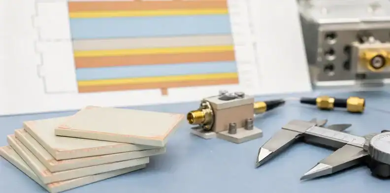
Dk and Df must be tied to frequency and method because dielectric values are not universal constants for every finished board. Material suppliers often publish values at stated frequencies and test conditions, while a finished PCB or ceramic circuit has geometry, copper, finish, and processing effects on top.
Rogers’ high-frequency material documentation is a useful reminder for RF buyers: dielectric properties are presented as material data for RF design, but the final stackup and construction still have to match the model. Ceramic substrates follow the same discipline. A catalog number is a starting point, not automatic proof that the fabricated line will meet the RF target.
The RF engineer should ask which value entered the simulation. Was it a material datasheet Dk, supplier design Dk, measured coupon value, or an adjusted field-solver value? Each one has a different use. Mixing them can make the prototype look like a fabrication problem when the real problem was an uncontrolled modeling assumption.
A named example makes the test-method distinction easier to check. The linked Rogers RO3000 laminate datasheet, page 2 lists the following RO3006 entries. This is ceramic-filled PTFE laminate, not a solid ceramic substrate; it illustrates how to read an RF material record, not an interchangeable ceramic choice.
| Entry for RO3006 in this PDF | Published value | Stated basis |
|---|---|---|
| Process Dk | 6.15 ± 0.15 | 10 GHz, 23°C; IPC-TM-650 2.5.5.5 |
| Design Dk | 6.50 | 8–40 GHz; differential phase length |
| Dissipation factor | 0.0020 | 10 GHz, 23°C; IPC-TM-650 2.5.5.5 |
These are typical-data entries in the cited document; its footnotes direct users to Rogers for specification values and describe design Dk as an average over tested lots and common thicknesses. The two Dk values do not by themselves measure frequency dispersion because their extraction methods differ. Do not average them or copy the design entry into a material acceptance limit.
Keep the exact PDF revision or saved copy with the model. If a product webpage, a laminate datasheet and a bondply document disagree, ask the material supplier which construction and revision apply before release. For a ceramic quote, require the same record fields: grade, material or circuit quantity, frequency, temperature, method, direction, nominal or guaranteed status, and the model in which the value is used.
For production, the purchase record should state whether the supplier may adjust trace width, ceramic thickness, conductor process, or finish. Any change near a controlled RF structure should return to engineering review.
A dielectric value is usable only when frequency, method, material grade, and construction are visible.
Which ceramic routes need the strictest dielectric review?
The strictness of dielectric review follows circuit sensitivity. A narrowband filter, a phase-matched path or a transition with little matching margin may require closer correlation than a less sensitive interconnect. LTCC identifies a co-fired construction, thin film describes metallization, and mmWave identifies an operating region; these labels alone do not rank the required review depth.
Orbray’s published LTCC information shows why the material system matters: its specific constrained-shrinkage process and compatible silver conductors support integrated RF structures. That supplier example does not assign a universal Dk or loss tangent to LTCC.
For a simple RF ceramic carrier, the buyer may only need material grade, thickness, conductor route, finish, and impedance target. For a 5G mmWave, radar, filter, or compact RF package, the buyer should request stronger review: dielectric data basis, dimensional tolerances, conductor process, via/cavity rules, and test method.
The RF/microwave ceramic PCB module article can help choose between LTCC, alumina, AlN, thin-film ceramic, and RF laminate. Once that route is chosen, this dielectric check tells the supplier what data must stay controlled.
The smaller and higher-frequency the RF structure, the less acceptable a generic ceramic Dk value becomes.
What should RF engineers send before the quote?
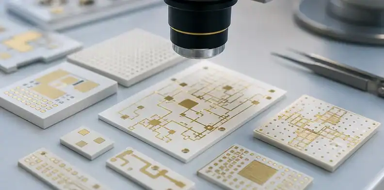
RF engineers should send the stackup, frequency band, impedance targets, dielectric values used in simulation, line geometry, reference planes, via structures, finish requirement, test method, and any no-change rules before the quote. Gerbers alone are not enough for a controlled RF ceramic build.
The file package should identify the design authority. If the RF model used a specific alumina, AlN, LTCC, or thin-film material assumption, that assumption should appear in the RFQ. If the supplier may propose alternatives, the RFQ should say what must be compared: Dk, Df, thickness, conductor process, finish, tolerance, and available evidence.
A short RFQ note can prevent confusion: “Please quote the ceramic RF substrate against the attached stackup and impedance table. State material grade, Dk/Df basis and frequency, ceramic thickness, conductor route, finish, tolerance limits, and any proposed change that affects the RF model.”
For layout-level review, use the QueenEMS RF ceramic PCB layout and DFM guide. The dielectric record should be settled before detailed layout exceptions are treated as manufacturing changes.
Do not release the RFQ until the dielectric value used in the model is traceable to the quoted construction.
How should suppliers document dielectric assumptions?
Suppliers should document dielectric assumptions in the quote, not only in email comments. A useful response states the ceramic material, nominal thickness, conductor route, finish, Dk/Df basis, tolerance, inspection method, and whether RF coupon or measurement data is included.
The quote should also separate typical data from controlled data. A typical material value may be enough for early screening. A controlled production build may need a supplier stackup record, impedance coupon, S-parameter measurement, dimensional report, or other evidence depending on the product.
Check how the model accounts for conductor roughness before changing Dk to fit a measurement. In its discussion of copper roughness and EM simulation, Rogers distinguishes a bulk dielectric input from an effective value that also represents roughness-related phase effects. Its explanation warns against supplying a roughness-adjusted value to a solver that is already calculating the same effect. This is a model-definition issue, not evidence that the ceramic itself has changed.
For a practical review, record three items beside the dielectric value: the structure used to extract it, whether conductor roughness was removed or included, and which roughness model is enabled in the simulation. If the supplier cannot answer, keep the input provisional. Do not silently switch between a material datasheet, a fitted circuit value and a solver library entry merely because one gives a closer curve.
When a prototype disagrees with the model, preserve the original material input and compare the measured construction first. Check dielectric thickness, finished conductor shape and the applicable metal surface data. Then document any change to the dielectric model separately from changes to geometry or roughness. Changing all three together can produce a fit without explaining which assumption was wrong. A revised model should reproduce another relevant structure or specimen before it becomes the purchasing basis; a single fitted line does not establish a transferable material property.
Change control belongs in the same record. The supplier should identify whether it may adjust trace width, dielectric thickness, conductor thickness, firing compensation, panel layout, finish, or equivalent material. For RF ceramic work, silent changes can shift impedance or resonance even when the board looks correct.
| Supplier response | Useful meaning |
|---|---|
| Material grade and thickness | Shows what construction is being quoted |
| Dk/Df basis and frequency | Connects material data to the RF model |
| Conductor route | Defines geometry, loss, and finish options |
| Tolerance and inspection | Shows whether the supplier can hold the design |
| RF evidence | Confirms whether the quote includes measurement support |
The supplier response should let RF engineering recreate the dielectric assumption without guessing.
How should buyers compare ceramic and RF laminate options?
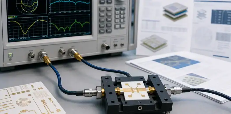
Buyers should compare ceramic and RF laminate options by the complete RF requirement: frequency, size, loss budget, heat, package integration, tolerance, assembly, and evidence. Ceramic is not always better; RF laminate is not always cheaper after the whole product is considered.
Ceramic may be stronger when the module is compact, high temperature, package-like, thermally dense, or needs stable small structures. RF laminate may be stronger when the product is board-level, connector-rich, larger, easier to assemble, or already qualified with a known laminate family.
The right comparison asks the same supplier questions for each route: material grade, dielectric basis, thickness, conductor process, finish, impedance tolerance, test evidence, lead time, and substitution control. A lower price is not comparable if it quietly changes the RF model.
QueenEMS can help overseas buyers turn that comparison into a quote-ready package for prototype and low-volume builds. The useful deliverable is not a generic “ceramic or laminate” answer; it is a controlled RFQ that says which assumptions can change and which must return to engineering.
Choose ceramic only when its package, heat, stability, or precision advantage matters more than the simpler RF laminate route.
FAQ
What is ceramic PCB dielectric constant?
It is the material property that shows how strongly the substrate affects electric fields. In RF design it influences impedance, wavelength, coupling, resonance, and physical line geometry.
Is lower dielectric constant always better for RF?
No. Lower Dk can reduce some sensitivities and support wider traces, but higher Dk can make compact structures possible. The right value depends on frequency, size, loss, and tuning goals.
What is dielectric loss in ceramic PCB?
Dielectric loss describes RF energy dissipated in the substrate, often expressed as Df or loss tangent. It contributes to insertion loss and heating, especially at microwave and mmWave frequencies.
Can I use datasheet Dk directly in a field solver?
Use it only as a starting point unless the datasheet frequency, method, thickness, and construction match the design. Ask the supplier for the design value or measurement basis used for the quoted stackup.
What should I ask a ceramic RF supplier?
Ask for material grade, Dk/Df basis, frequency, thickness, conductor route, finish, tolerance, RF coupon or test support, and which process changes require approval.
Send QueenEMS a ceramic RF dielectric review package
To discuss a dielectric-data gap, send QueenEMS the current model inputs with the source documents and proposed stack. Identify the frequency range, permitted substitutions and acceptance question. The response should distinguish an available material record from additional characterization the project still needs.
Sources
- Rogers Corporation, High Frequency Circuit Materials
- Orbray: LTCC materials and processing
Written by the QueenEMS Engineering Team
Upload your files today · Free DFM check before production · Ship worldwide
Get your PCB prototypes in as fast as 24 hours. We handle FR4, Rogers, and Flex up to 60 layers — free prototypes for 2–4 layer boards, no minimum order.
Just upload your Gerber + BOM — we source every part, assemble, and inspect (AOI + X‑Ray) so you don't have to chase suppliers. Boards ship in as fast as 24 hours.