
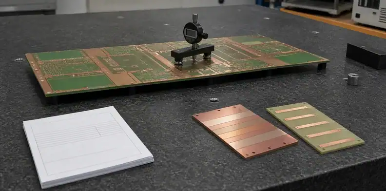
Quick Answer: Hybrid PCB warpage control should start before fabrication by checking material symmetry, copper balance, press construction, thickness, panel support, and the receiving measurement rule. The buyer should separate ordinary bow/twist acceptance from the special risk created when a mixed-material stackup has uneven CTE, copper distribution, or local RF features.
Key takeaways
- Warpage prevention starts with stackup and copper balance, not with receiving inspection alone.
- Mixed materials can bend differently after pressing, routing, surface finish, baking, or assembly heat.
- The quote should state how bow and twist will be measured and who accepts any deviation.
- A board that meets a generic limit may still be unsafe for fine-pitch assembly or connector fit.
A hybrid PCB can be electrically correct and still create trouble when the bare board is not flat enough for assembly, connector seating, fixture fit, or enclosure alignment. The usual bow and twist question becomes sharper when a low-loss or ceramic-filled dielectric is combined with FR4, asymmetric copper, heavy ground areas, cavities, or edge-launch geometry.
This article does not replace the general PCB bow and twist acceptance page. That page owns the basic acceptance concept. This page owns the mixed-material release decision: what to check before quote, what evidence to ask for, and when warpage risk should hold the order before assembly.
Table of Contents
- Find the real flatness risk in the stackup
- Check copper balance before blaming the factory
- Review press and cooling assumptions
- Connect panel design to final board flatness
- Define how bow and twist will be measured
- Keep receiving evidence tied to the release rule
- Judge assembly impact before accepting a deviation
- Write the warpage boundary into the RFQ
Find the real flatness risk in the stackup
The first review should ask whether the stackup is mechanically balanced enough for the product. Hybrid boards often place a low-loss material only where RF performance needs it, while other layers use FR4 for cost and routing density. That can be practical, but the construction may pull unevenly when pressed, cooled, routed, finished, or heated during assembly.
Ask the supplier to mark the material locations, dielectric thicknesses, copper weights, heavy copper zones, cavities, and plated areas that could affect flatness. A board with the same total thickness can behave differently when the material order changes. The high-frequency hybrid PCB stackup RFQ page covers the electrical stackup request; this page uses that stackup to judge flatness risk.
| Risk feature | Why it matters | Buyer question |
|---|---|---|
| One-sided low-loss core | Creates uneven expansion response | Can the stackup be balanced? |
| Heavy copper on one side | Pulls during thermal cycles | Can copper be balanced or relieved? |
| Thin long board | More sensitive to process stress | Is panel support enough? |
| Edge connector area | Fit may be stricter than generic limit | Does assembly accept the flatness rule? |
Flatness rule: Review warpage risk from the released construction, not from board thickness alone.
A good review also separates local and global flatness risk. A whole panel may measure acceptably while a connector area, shield can zone, or narrow board tail lifts enough to hurt assembly. Ask which area matters to the product, not only which measurement is easiest to report.
For a long or thin product, the buyer should share enclosure, connector, or fixture constraints with the fabricator. The supplier cannot protect a fit requirement it cannot see. That extra context often changes the panel support or flatness evidence request before fabrication starts.
Check copper balance before blaming the factory
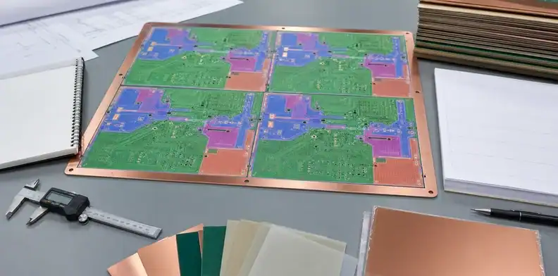
Copper balance is one of the most practical buyer checks because it is visible in design data. A large ground plane, uneven copper pour, plated features, or copper thieving decision can change how the board responds to press and heat. The supplier can compensate within limits, but it should not silently change functional copper without design approval.
Ask CAM to identify whether copper imbalance creates a manufacturing concern. If dummy copper, thieving, or local copper adjustment is proposed, engineering should confirm the change does not affect RF fields, impedance, creepage, or thermal behavior. Purchasing should record whether the adjustment is part of the quoted fabrication data.
Do not treat copper balance as a cosmetic issue. It can affect solder printing, component coplanarity, connector seating, and long-term handling. On a hybrid board, the copper decision may also interact with material placement.
Copper call: Let the supplier propose manufacturable copper balance, but keep functional copper changes under engineering approval.
The buyer should also separate intentional copper from balancing copper. Functional planes, shields, launch grounds, thermal copper, and return paths should not be moved casually. Manufacturing balancing copper can be helpful, but it must avoid impedance fields, isolation areas, creepage zones, and mechanical keep-outs.
When the supplier recommends copper changes, ask for a marked CAM view or note showing what changes are proposed. Engineering can then approve the manufacturing help without losing control of the actual circuit behavior.
Review press and cooling assumptions
Warpage can begin in the press cycle. Material cure behavior, pressure distribution, cooling rate, panel load, bondply flow, copper pattern, and board thickness all affect the final shape. The buyer does not need to own the press recipe, yet the quote should state whether the construction is inside the supplier’s normal hybrid process window.
A useful supplier reply will not promise zero movement. It will explain whether the stackup is balanced, whether any build adjustment is recommended, and whether first-lot flatness measurement is included. That answer helps the buyer decide whether a prototype is safe to release or whether a small first article build should come first.
When the proposed construction has a material or press-cycle concern, connect the decision to the hybrid PCB lamination and CTE review. Flatness is one visible result of that broader process risk.
Press signal: A supplier should flag abnormal press or cooling risk before the PO, not after the board is already warped.
This is a judgment boundary, not an attempt to audit every press setting. The supplier owns the process recipe. The buyer owns release of a construction that may be outside the supplier’s normal window. A useful quote answer says whether the stackup is normal, needs adjustment, or should be built as a first lot before volume.
When several suppliers quote the same design, compare whether each one notices the flatness risk. A low price with no comment may simply mean the review was shallow. A slightly higher quote that identifies panel support and first-lot measurement may be the safer production answer.
Connect panel design to final board flatness
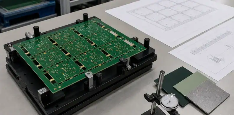
Panelization can protect or worsen flatness. Rail design, tab placement, routing sequence, v-score use, carrier support, and copper distribution in the panel can change how the finished board relaxes after separation. A small RF board may look stable in the panel but twist after depaneling if the support strategy is weak.
Ask whether the quoted panel drawing supports the board until the last safe manufacturing step. If the supplier proposes a tab, rail, or routing change, engineering should review whether it affects RF edges, connector clearance, mounting holes, or assembly handling. A panel solution that damages the functional edge is not a solution.
| Panel factor | Flatness effect | Approval owner |
|---|---|---|
| Rail width | Supports thin boards through process | Supplier proposes, buyer reviews |
| Tab placement | Controls release stress | Engineering reviews keep-outs |
| Routing sequence | Affects relaxation after cutout | Supplier controls within approval |
| V-score use | May induce stress on some shapes | Engineering and assembly approve |
Panel point: Flatness evidence should include how the board is supported and separated, not only the final board outline.
Define how bow and twist will be measured
Measurement rules avoid disputes. The quote should state the acceptance reference, measurement method, sample plan, and whether the limit applies at shipment, receiving, or after a specified handling step. A board can look acceptable by eye and still fail a fixture or fine-pitch assembly process.
Do not let the supplier and buyer use different surfaces, support points, or sample conditions. Quality should decide how incoming boards will be checked. Engineering should state whether the generic flatness limit is enough for connectors, BGAs, sockets, shielding cans, or housing fit.
Some products need a tighter practical limit than the default class rule. Others can accept a minor deviation if assembly tooling holds the board flat. The decision should be made before shipment, not during a receiving argument.
Measurement check: A warpage limit is useful only when the measurement condition and assembly consequence are both visible.
Put that measurement rule in the same folder as the stackup and panel drawing so future lots use the same acceptance basis.
Record the measurement condition in language that receiving can use. State whether boards are measured after unpacking, after a bake, after depaneling, or before assembly loading. Those conditions can matter when moisture, packaging pressure, or support rails affect the shape.
Quality should keep photos only as support, not as the main proof. The measurement method and disposition decide acceptance. Photos help explain a disputed board, but they do not replace a defined flatness rule.
Keep receiving evidence tied to the release rule
Receiving inspection should not create a new standard after the boards arrive. The receiving team should use the same bow/twist method, support condition, and acceptance limit that purchasing released with the RFQ or PO. When the method changes at the dock, a supplier dispute can become a process argument instead of a board decision.
The useful record is simple: lot number, drawing revision, measured samples, board support condition, measured result, photo support, and disposition. If the board is accepted with a concession, the record should say whether that concession applies only to the current shipment. If the board is rejected, the record should show which released rule it failed.
This matters most when the schedule is tight. A buyer may be tempted to accept a slightly warped lot because assembly is waiting. That decision can be reasonable only when the assembly owner confirms the fixture, solder process, connector fit, and enclosure need. Receiving can document the condition; engineering and assembly should decide whether it can be used.
Receiving record: Keep the measurement proof tied to the released hybrid PCB warpage rule, not to a new inspection habit created after delivery.
The same record helps repeat orders. If a later lot changes thickness, panel size, copper balance, or packaging pressure, the team can compare the new evidence with the old acceptance basis instead of reopening the whole flatness debate.
Judge assembly impact before accepting a deviation
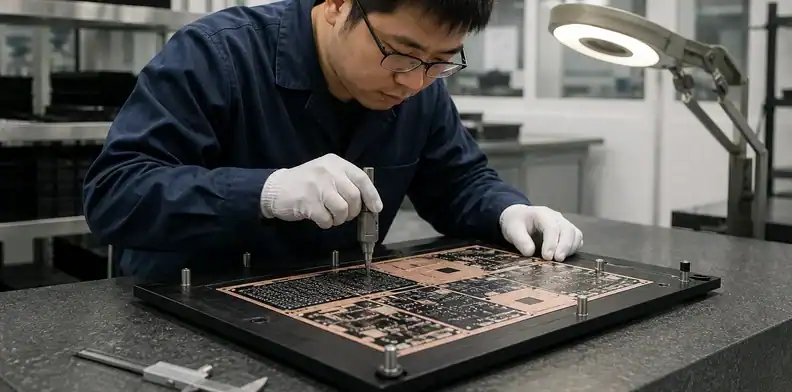
Accepting a flatness deviation is not only a quality decision. Assembly may face solder paste variation, component tilt, BGA coplanarity trouble, connector seating force, selective solder issues, or fixture mismatch. A bare-board supplier may view a minor warp as acceptable while the assembler sees a real yield risk.
For PCBA orders, ask the assembly side to review the deviation before acceptance. That is especially true when the board is long and thin, has fine-pitch parts, uses heavy connectors, or must fit a mechanical enclosure. A small bare-board concession can become an expensive assembly delay.
If the order is bare PCB only, purchasing should still record the intended assembly condition. The next buyer or assembler will need to know whether the board was accepted as-is or under a specific handling assumption.
Assembly call: Do not accept a hybrid PCB warpage deviation until the assembly or fit consequence is known.
Receiving teams should avoid making this decision alone. They can measure and document the board shape, but the assembly owner knows whether solder printing, component placement, connector insertion, or enclosure loading will tolerate it. That split is especially useful when the board is needed urgently and the supplier asks for concession.
If the decision is to accept, record whether the concession applies only to that lot. A one-time acceptance after visual and fixture review is different from changing the production flatness requirement.
Write the warpage boundary into the RFQ
The RFQ should attach the stackup, board outline, panel preference, assembly constraints, flatness requirement, and evidence request. It should also ask the supplier to flag any stackup or panel change recommended to reduce warpage. That turns the issue into a manufacturing decision instead of a receiving surprise.
A practical RFQ sentence is: “Please review hybrid stackup flatness risk before quote; state bow/twist acceptance, panel support assumptions, copper-balance changes, and any condition that requires buyer approval before fabrication.” This gives the supplier freedom to improve manufacturability while protecting released design intent.
RFQ rule. Put the flatness boundary in the quote before build, because the cheapest correction is often a stackup or panel decision made early.
The RFQ should also state whether the buyer wants a measurement report for every lot or only for first production. Lot-by-lot reports may be useful during supplier launch, while a stable repeat build may only need the supplier to keep records unless a change occurs.
For a bare-board-only order, the buyer can still protect assembly by stating the expected assembly process. Mention fine-pitch SMT, press-fit connectors, mechanical sockets, thermal interface pads, or enclosure alignment when they drive the flatness requirement. The fabricator can then propose a panel or stackup adjustment that respects the end use.
For a PCBA order, ask the assembler and fabricator to agree on the hold point. A board that is barely acceptable as a bare PCB may become risky after solder reflow. The release decision should state whether flatness is checked before assembly, after assembly, or both.
If your PCB or PCBA project has mixed materials, flatness risk, connector fit, fine-pitch assembly, or receiving acceptance questions, send QueenEMS the stackup, panel drawing, outline, assembly constraints, and required flatness rule through the contact page. QueenEMS can help review whether the quote protects both fabrication and assembly release.
Sources
FAQ
Is hybrid PCB warpage only a supplier quality problem?
No. Supplier process matters, but stackup symmetry, copper balance, board shape, panel design, and assembly constraints can create the risk before fabrication starts.
Can a board pass a standard bow/twist limit and still fail assembly?
Yes. A generic limit may not protect fine-pitch placement, connector seating, socket fit, or enclosure alignment. Assembly impact should be part of the decision.
Should copper thieving be allowed to reduce warpage?
Sometimes. It can help manufacturability, but engineering must approve changes near RF, impedance, creepage, thermal, or functional copper areas.
What should be saved after accepting a deviation?
Save the measured result, method, sample condition, assembly review, disposition, and whether the same condition is allowed on repeat orders.
If your PCB or PCBA project has mixed materials, flatness risk, connector fit, fine-pitch assembly, or receiving acceptance questions, send QueenEMS the stackup, panel drawing, outline, assembly constraints, and required flatness rule through the contact page. QueenEMS can help review whether the quote protects both fabrication and assembly release.
Written by the QueenEMS Engineering Team
Upload your files today · Free DFM check before production · Ship worldwide
Get your PCB prototypes in as fast as 24 hours. We handle FR4, Rogers, and Flex up to 60 layers — free prototypes for 2–4 layer boards, no minimum order.
Just upload your Gerber + BOM — we source every part, assemble, and inspect (AOI + X‑Ray) so you don't have to chase suppliers. Boards ship in as fast as 24 hours.