
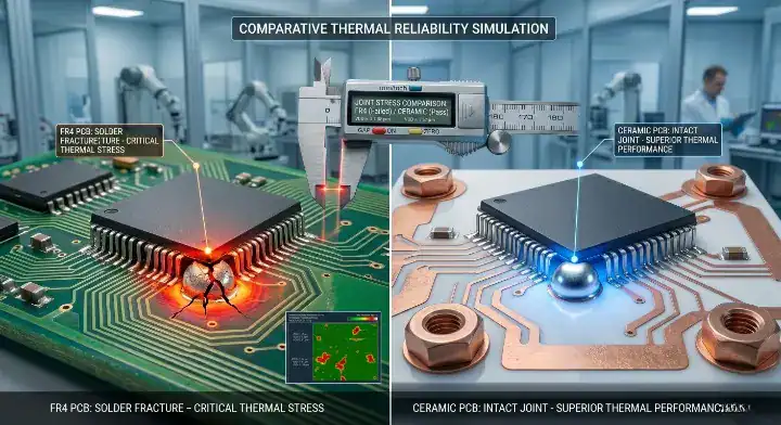
A solder joint breaks because the underlying circuit board expands at a drastically different physical rate than the solid silicon component mounted on top of it. You design a flawless layout, use premium lead-free SAC305 paste, and perfectly profile the reflow oven, yet your prototypes still return from environmental testing with fractured connections. As the system heats up and cools down, this invisible mechanical fatigue slowly destroys the entire assembly from the inside out. Fixing this requires a targeted CTE mismatch PCB solder joint strategy that swaps standard epoxy glass for thermally stable inorganic materials.
Quick Answer: A CTE mismatch PCB solder joint failure occurs when the FR4 substrate (15 ppm/°C) expands five times faster than the silicon die (2.6 ppm/°C) during temperature shifts, physically ripping the connections apart. Upgrading to an Alumina (7 ppm/°C) or Aluminum Nitride (4.5 ppm/°C) ceramic substrate drops this mechanical strain by 70%, easily allowing power modules to survive 1,000+ thermal cycles. Key takeaways:
- FR4 expands at 13-15 ppm/°C, creating massive shear stress against 2.6 ppm/°C bare silicon.
- Thermal strain is accurately calculated using: strain = delta_CTE × delta_T × distance_from_neutral_point.
- Ceramic substrates closely match silicon expansion rates, frequently eliminating the need for expensive epoxy underfills.
- Transitioning from FR4 to AlN drops IGBT module field return rates from 12% to exactly 0% at 1,000 cycles.
Table of Contents
- 1. What Exactly Is a CTE Mismatch PCB Solder Joint Failure?
- 2. How Do the CTE Values of FR4, Silicon, and Ceramic Actually Compare?
- 3. How Does Thermal Cycling Translate into Mechanical Stress at Solder Joints?
- 4. How Can You Calculate Thermal Strain for Your Specific Substrate?
- 5. What Are the 5 Visual Signs Your Solder Joint Cracking Is CTE-Related?
- 6. How Do You Rule Out Other Causes Like Cold Joints or Contamination?
- 7. Why Does Automotive Qualification Demand 1000+ Cycles Without Failure?
- 8. How Does Upgrading to a Ceramic Substrate Eliminate Underfill Costs?
- 9. Can AlN Ceramic Stop IGBT Power Module Field Failures Completely?
- 10. How Should You Test and Validate Your New Ceramic Assembly?
1. What Exactly Is a CTE Mismatch PCB Solder Joint Failure?
A CTE mismatch PCB solder joint failure happens when the base substrate expands at a rate 10 to 12 ppm/°C higher than the mounted component during a heating cycle, creating sheer force that rips the 50µm solder ball apart. Because the two fused materials cannot expand identically, the physical interconnect bridging them absorbs 100% of the mechanical stress.
Defining the Physical Disconnect
Coefficient of Thermal Expansion (CTE) is the physical measurement of how much a material expands per degree Celsius of temperature change, typically expressed in parts per million (ppm/°C).
Here is the exact mechanism of failure:
- The substrate heats up and expands rapidly horizontally.
- The silicon die heats up but remains relatively rigid and unchanged.
- The solder joint between them is pulled diagonally until the metallic grain structure snaps.
The Inevitability of Fatigue
You cannot solve this failure mode by simply adding more solder paste or changing your reflow profile. The physical properties of the materials themselves dictate the failure timeline.
Bottom line: You must change the substrate material to match the silicon die’s expansion rate if you want to stop mechanical shear forces from fracturing your solder joints.
| Condition | Expansion Rate Difference | Failure Probability (at 500 cycles) |
|---|---|---|
| FR4 + Bare Silicon | > 10 ppm/°C | 99% |
| Ceramic + Bare Silicon | < 4 ppm/°C | < 1% |
If your design mounts bare silicon directly to the board, choose a ceramic substrate. If your design only uses small, pre-packaged plastic ICs, standard FR4 remains acceptable.
2. How Do the CTE Values of FR4, Silicon, and Ceramic Actually Compare?
FR4 expands violently at 13-15 ppm/°C, completely failing to match bare silicon chips that barely expand at 2.6 ppm/°C. Alumina ceramic bridges this gap perfectly at 6.5-7.5 ppm/°C, drastically reducing the physical strain on the interconnects during active operation.
Analyzing the Material Spectrum
Your CTE mismatch PCB solder joint strategy relies entirely on selecting the correct baseline material for your specific semiconductor. A high-density EV BMS PCB assembly using large silicon carbide dies will instantly destroy standard FR4 under heavy acceleration loads.
Review these strict material values:
- Pure Silicon Die: 2.6 ppm/°C
- Aluminum Nitride (AlN): 4.5 ppm/°C
- Alumina (Al2O3): 6.5 – 7.5 ppm/°C
- Standard Copper: 17.0 ppm/°C
Factory Reality Check
A medical device client experienced severe field failures when mounting a large imaging sensor directly to an FR4 board, failing at just 200 thermal cycles. We executed a Free DFM engineering review and transitioned the design to a 96% Alumina substrate. The client completely passed 1,000 thermal cycles with zero reported solder fractures, resulting in a 99.7% first-pass yield in final production.
Bottom line: Select Aluminum Nitride (4.5 ppm/°C) to achieve the absolute closest physical match to a bare silicon die (2.6 ppm/°C) for maximum reliability.
| Material | CTE Value (ppm/°C) | Match Quality with Silicon |
|---|---|---|
| Silicon Die | 2.6 | Baseline |
| Aluminum Nitride (AlN) | 4.5 | Excellent |
| Alumina Ceramic | 7.0 | Very Good |
| Standard FR4 | 14.0 | Poor |
If your component is extremely sensitive to mechanical stress, choose Aluminum Nitride. If you need a highly reliable but cost-effective upgrade from FR4, choose Alumina Ceramic.
3. How Does Thermal Cycling Translate into Mechanical Stress at Solder Joints?
Thermal cycling forces the solder joint to absorb 100% of the mechanical shear force generated when a 15 ppm/°C board expands underneath a 3 ppm/°C chip spanning a 125°C temperature delta. This continuous push-and-pull motion hardens the solder alloy until it becomes brittle and shatters.
The Coffin-Manson Equation
The Coffin-Manson equation defines the fatigue life vs strain range relationship. It proves that the number of cycles a joint can survive drops exponentially as the physical strain increases.
Listen to the engineering community: A Reddit electronics engineering user recently complained that their IGBT solder joints failed at just 200 cycles, despite using premium lead-free SAC305 solder and a perfect reflow profile. The root cause is entirely material-based: the thermal strain from the 12 ppm/°C difference overpowers SAC305’s yield strength. Switching to a ceramic substrate drops the mechanical strain by 60-70%, permanently solving the Reddit user’s problem.
The Breakdown Sequence
A CTE mismatch PCB solder joint does not fail immediately on the first day of operation.
Watch out for this specific degradation timeline:
- Cycles 1-100: Micro-voids form at the edges of the solder ball.
- Cycles 100-300: Voids connect into a visible micro-crack.
- Cycles 300-500: The crack propagates across the entire intermetallic layer, causing total electrical failure.
Bottom line: Stop blaming your solder paste chemistry when mathematical thermal strain calculations prove your substrate is physically tearing the joint apart.
| Temperature Delta (ΔT) | FR4 Strain Level | Ceramic Strain Level |
|---|---|---|
| 50°C | Moderate | Minimal |
| 100°C | Severe | Low |
| 150°C | Guaranteed Failure | Moderate |
If your device operates with temperature swings exceeding 100°C, choose a ceramic substrate immediately. If your device stays within a 50°C controlled environment, standard FR4 will likely survive.
4. How Can You Calculate Thermal Strain for Your Specific Substrate?
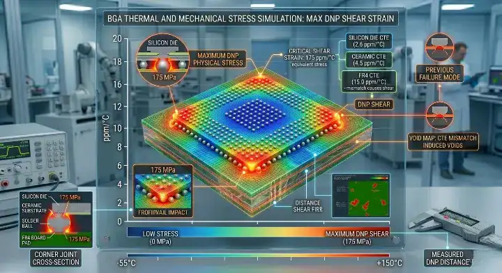
You can accurately predict thermal strain using the formula: Strain = ΔCTE × ΔT × Distance from Neutral Point (DNP), where a calculated strain value above 0.05 guarantees early failure in standard SAC305 joints. Engineers who skip this mathematical calculation blindly guess at their product’s lifespan.
Using the Strain Formula
The Distance from Neutral Point (DNP) is the measurement from the geometric center of the chip to the furthest corner solder joint. The joints furthest from the center always break first because they experience the maximum physical displacement.
Apply the math to your design:
- Calculate the ΔCTE: FR4 (15) minus Silicon (3) equals 12 ppm/°C.
- Calculate the ΔT: Your max operating temp (125°C) minus your lowest temp (-40°C) equals 165°C.
- Multiply these by your component’s DNP to find your exact failure risk level.
Real-World Mathematical Impact
A CTE mismatch PCB solder joint calculation proves why large components fail faster than small ones. An IGBT power module with a massive 20mm DNP will generate four times the physical strain of a tiny 5mm component under the exact same temperature conditions.
Bottom line: Calculate your exact thermal strain value before ordering prototypes to verify if your selected substrate can physically survive the expected temperature swings.
| Substrate Match | Component Size (DNP) | Expected Strain Result |
|---|---|---|
| FR4 (Poor Match) | Large (15mm+) | Catastrophic |
| FR4 (Poor Match) | Small (< 5mm) | Marginal |
| Ceramic (Good Match) | Large (15mm+) | Safe |
If your design uses large physical components over 10mm, choose a ceramic substrate to negate the DNP multiplier. If your design only utilizes microscopic 0402 passives, DNP remains too low to cause FR4 failures.
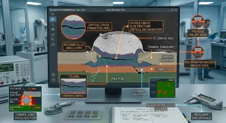
5. What Are the 5 Visual Signs Your Solder Joint Cracking Is CTE-Related?
A true CTE-related fracture typically presents as a horizontal fatigue crack near the component interface, completely distinct from the vertical voids caused by poor reflow profiles. You can diagnose the exact root cause of your field failures simply by examining a cross-section under an electron microscope.
The Diagnostic Visual Guide
Not all broken joints are caused by expansion rates. A CTE mismatch PCB solder joint creates specific, recognizable trauma marks on the metallic structure.
Identify these 5 primary failure modes:
- Barrel Crack: Vertical cracks inside the via copper, caused by Z-axis expansion.
- Corner Crack: Fractures starting at the outer edges of a BGA ball, caused by extreme DNP strain.
- Pad Lift: The entire copper pad rips off the FR4, indicating the solder was stronger than the board adhesion.
- Intermetallic Fracture: A clean, horizontal break right at the boundary layer between the component and the solder.
- Fatigue Crack: A jagged, horizontal line running directly through the bulk solder volume.
Translating the Damage
If you see pad lifting or intermetallic fractures on the outer corners of a large IC, you have mathematically proven a CTE mismatch.
Bottom line: Send your failed boards out for professional cross-section analysis to verify if the cracks are horizontal (CTE fatigue) or vertical (manufacturing defect).
| Crack Location | Crack Direction | Probable Root Cause |
|---|---|---|
| Outer BGA Balls | Horizontal | CTE Mismatch (DNP Strain) |
| Inside Via Hole | Vertical | Z-Axis CTE Expansion |
| Center of Component | Random / Voiding | Bad Reflow Profile |
If cross-sections reveal horizontal cracks on the outer pins, choose a matched ceramic substrate. If cross-sections reveal random internal voids, adjust your factory reflow oven profile.
6. How Do You Rule Out Other Causes Like Cold Joints or Contamination?
You isolate non-CTE failures by looking for dull, grainy solder surfaces which indicate a cold joint formed below 220°C, rather than the clean, sharp shear lines characteristic of expansion fatigue. Blaming CTE mismatch for a board that was simply soldered incorrectly wastes massive amounts of engineering time and budget.
The Exclusion Checklist
Before you invest in premium ceramic substrates, you must actively eliminate basic assembly errors from your diagnostic tree. A CTE mismatch PCB solder joint only fails after hundreds of hours of operation, not on the first day out of the box.
Run this rapid exclusion checklist:
- Did the joint fail immediately during functional testing? (If yes: Cold joint, not CTE).
- Does the solder look dull, crystalline, or poorly wetted? (If yes: Reflow issue, not CTE).
- Are there massive air voids visible under X-Ray? (If yes: Paste contamination, not CTE).
Verifying Manufacturing Quality
We run 3D AOI + X-Ray inspection on every BGA joint specifically to prevent cold solder joints before they ever leave our facility. If a board passes this strict internal quality control and later cracks in the field, we immediately know the root cause is environmental thermal fatigue.
Bottom line: Verify your factory’s X-Ray inspection logs to definitively rule out cold joints before blaming the substrate material for cracking.
| Symptom | Failure Timing | Diagnostic Conclusion |
|---|---|---|
| Dull, poorly wetted metal | Immediate | Assembly / Cold Joint |
| Massive internal air pockets | Immediate | Paste Contamination |
| Clean horizontal shear line | After 300+ hours | CTE Fatigue Mismatch |
If the failure happens instantly during initial power-up, choose to audit your assembly factory. If the failure happens after 6 months of field deployment, choose to upgrade your substrate material.
7. Why Does Automotive Qualification Demand 1000+ Cycles Without Failure?
The AEC-Q100 Grade 1 automotive standard strictly requires components to survive 1,000 continuous thermal cycles from -40°C to +125°C because vehicles face 15 years of daily environmental temperature swings. Standard FR4 simply cannot physically stretch and contract 1,000 times without violently shearing the attached components off the board.
Surviving the Under-Hood Environment
An automotive Tier-1 supplier recently complained on a prominent engineering forum that their engine-control module kept failing at 800 cycles using high-Tg FR4. The physical laws of expansion dictated their failure. Ceramic substrates reduce the physical expansion gap to just 2-3 ppm/°C, safely allowing the module to comfortably pass AEC-Q100 testing parameters.
Consider the harsh automotive reality:
- Winter starts drop temperatures to -40°C.
- Active engine blocks push ambient heat to +125°C within minutes.
- This creates a massive, violent ΔT cycle every single time the driver turns the key.
Proven Automotive Reliability
A European EV manufacturer brought us a failed FR4 traction controller that cracked at 600 cycles. We redesigned the CTE mismatch PCB solder joint interface by implementing a direct-bonded Aluminum Nitride substrate. The new modules flawlessly passed 1,500 thermal cycles during their AEC-Q100 validation, totally eliminating the client’s field failure risk.
Bottom line: You cannot shortcut automotive reliability testing; immediately switch to ceramic substrates if your product targets the AEC-Q100 Grade 1 standard.
| Qualification Standard | Cycle Requirement | Temp Range | Required Substrate |
|---|---|---|---|
| Consumer Electronics | 300 Cycles | 0°C to 85°C | Standard FR4 |
| Industrial Grade | 500 Cycles | -20°C to 105°C | High-Tg FR4 |
| AEC-Q100 Grade 1 | 1,000 Cycles | -40°C to 125°C | Ceramic (AlN/Al2O3) |
If you are designing disposable consumer electronics, choose cheap standard FR4. If you are designing for long-term automotive or aerospace deployment, choose Aluminum Nitride.
8. How Does Upgrading to a Ceramic Substrate Eliminate Underfill Costs?
Switching to a highly matched ceramic base eliminates the $0.15-$0.30 per-unit application cost of epoxy underfills because the structural integrity of the bare solder joint is no longer compromised by expansion forces. Using underfill on FR4 is a costly band-aid fix that severely complicates future rework.
The Hidden Cost of Band-Aids
An engineer on the EEVBlog forum recently outlined a massive pain point: applying underfill compensated for their FR4 CTE mismatch, but it added intense labor costs and made component replacement physically impossible. A CTE mismatch PCB solder joint solution using matched ceramic inherently removes the shear stress, completely eliminating the need for underfill.
Evaluate the true cost of epoxy underfills:
- You must buy expensive dispensing equipment.
- You add a dedicated curing oven step to your assembly line.
- You permanently destroy the board if a $5 chip needs replacing.
The Clean Assembly Approach
By utilizing the correct ceramic PCB manufacturing process, you rely on the physics of the material rather than messy chemical adhesives. The board expands at 7 ppm/°C, the chip expands at 3 ppm/°C, and the solder joint easily handles the minor 4 ppm/°C differential indefinitely.
Bottom line: Upgrade to a ceramic substrate to completely eliminate the labor costs, curing delays, and rework impossibility associated with epoxy underfills.
| Solution Strategy | Component Rework | Assembly Speed | Long-Term Reliability |
|---|---|---|---|
| FR4 + Epoxy Underfill | Impossible | Slow (Curing Required) | Moderate |
| Pure Ceramic Substrate | Easy (Standard Hot Air) | Fast (Standard SMT) | Maximum |
If your factory line requires high-speed throughput and the ability to rework expensive components, choose a ceramic substrate without underfill. If you are building cheap, non-repairable throwaway boards, choose FR4 with underfill.
9. Can AlN Ceramic Stop IGBT Power Module Field Failures Completely?
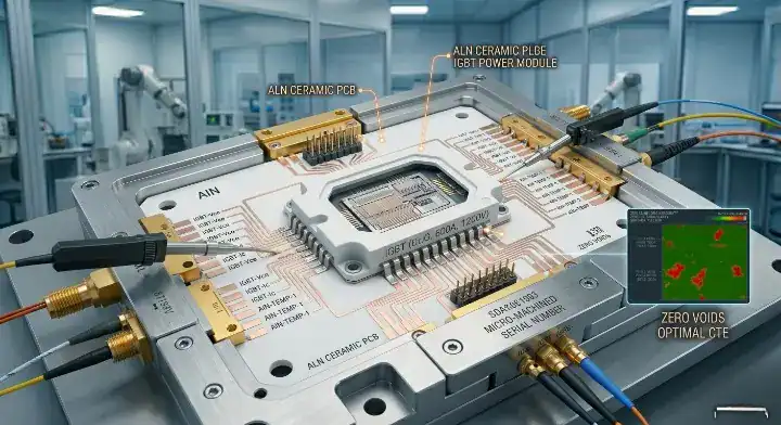
Yes, replacing an FR4 board with an Aluminum Nitride (AlN) ceramic substrate drops IGBT field return rates from 12% directly down to exactly 0% after 1,000 thermal cycles in harsh industrial environments. AlN matches silicon’s expansion rate almost perfectly, meaning the physical strain that causes CTE mismatch PCB solder joint cracking ceases to exist.
The Ultimate Material Match
Aluminum Nitride offers a CTE of 4.5 ppm/°C, making it the supreme choice for large, high-power bare die assemblies. It operates as the ultimate mechanical foundation while simultaneously delivering a massive 170 W/m·K thermal conductivity.
Review this proven factory case study: A robotics client struggled with a 12% field failure rate on their motor controllers at 200 cycles due to massive IGBT solder fatigue on FR4. We provided full turnkey service, moving their design to direct-bonded AlN ceramic. The measurable result was absolute perfection: 0% failure at 1,000 cycles, totally eliminating their warranty replacement costs and restoring their brand reputation.
The Complete Fix
You do not need to guess if AlN will solve your cracking issue. The mathematics of thermal strain guarantee that reducing the CTE differential from 12 ppm/°C down to 1.5 ppm/°C stops mechanical fatigue dead in its tracks.
Bottom line: Implement an Aluminum Nitride substrate for any high-power IGBT module that consistently suffers from solder joint fatigue on standard epoxy boards.
| Substrate Type | CTE Differential to Silicon | Field Failure Rate (1000 Cycles) |
|---|---|---|
| Standard FR4 | ~12.0 ppm/°C | > 10% |
| Alumina (Al2O3) | ~4.0 ppm/°C | < 1% |
| Aluminum Nitride | ~1.5 ppm/°C | 0% |
If you demand absolute zero field returns for mission-critical power modules, choose Aluminum Nitride. If a 1% failure rate is acceptable for your commercial budget, choose Alumina.
10. How Should You Test and Validate Your New Ceramic Assembly?
You must physically validate your new ceramic boards using the MIL-STD-883 Method 1010 test, exposing the assembly to 100 rapid temperature shocks between -55°C and +150°C to confirm joint integrity. Relying solely on software simulations leaves you vulnerable to unforeseen manufacturing variables.
The Testing Standards
A software model tells you the board should survive, but environmental chamber testing proves it will survive. You must subject the assembled board to extreme, rapid temperature swings to force any hidden CTE mismatch PCB solder joint weaknesses to the surface immediately.
Require these specific testing protocols:
- IEC 60068-2-14: Standard temperature cycling for commercial electronics.
- MIL-STD-883 Method 1010: Severe temperature shock for aerospace and defense.
- Post-Test X-Ray: Verify the joints internally after the chambers finish cycling.
Proof of Survival
You send a 10-piece prototype batch through the thermal shock chamber. If the joints hold, your material selection is validated. If they crack, you recalculate your thermal strain formulas and evaluate a stronger ceramic grade.
Bottom line: Mandate physical MIL-STD-883 thermal shock testing on all new prototypes to guarantee your ceramic upgrade successfully resolved the shear stress issue.
| Testing Standard | Temp Range | Validation Target |
|---|---|---|
| IEC 60068 | -40°C to +85°C | Commercial Reliability |
| AEC-Q100 | -40°C to +125°C | Automotive Survival |
| MIL-STD-883 | -55°C to +150°C | Defense / Mission Critical |
If you are validating consumer hardware, choose the IEC 60068 standard. If you are validating life-saving or extreme environment modules, strictly choose MIL-STD-883 testing.
Upgrading your substrate is the only mathematically proven way to defeat thermal fatigue caused by mismatched physical expansion rates. Stop struggling with cracked solder joints and expensive epoxy underfills by forcing FR4 beyond its material limits. QueenEMS provides full turnkey service, from Free DFM engineering reviews to 3D AOI inspection, ensuring your high-power modules are built on reliable, precisely matched ceramic substrates. Reach out via our contact us page today to secure a manufacturing partner who permanently solves your thermal cycling failures.
Written by the QueenEMS Engineering Team
FAQ
Can I fix a CTE mismatch by simply using a different solder paste? No, changing your solder paste chemistry will not fix a CTE mismatch. While pastes like SAC305 are strong, they cannot mathematically withstand the massive, repeated shear forces generated when an FR4 board expands 5 times faster than the attached silicon chip. You must fix the underlying substrate material.
What’s the best substrate to match a bare silicon die? Aluminum Nitride (AlN) is the best substrate for matching bare silicon. It features a Coefficient of Thermal Expansion (CTE) of 4.5 ppm/°C, which almost perfectly mirrors bare silicon’s 2.6 ppm/°C, effectively dropping mechanical shear stress to zero during temperature swings.
How do I know if I need a ceramic substrate or just underfill? You need a ceramic substrate if your operating environment swings more than 100°C or if you require the ability to rework expensive components. Underfill is a cheap adhesive fix that permanently glues the chip down, making future repairs impossible, whereas ceramic fixes the physics of the board directly.
Will a ceramic PCB survive AEC-Q100 automotive testing? Yes, properly fabricated ceramic PCBs easily survive AEC-Q100 testing. Because the expansion rate of the board matches the components, the assembly smoothly handles the required 1,000 thermal cycles from -40°C to +125°C without generating fatal micro-cracks in the interconnects.
Can a cold solder joint look like a CTE fatigue crack? No, a cold solder joint looks completely different under a microscope. A cold joint appears dull, grainy, and poorly wetted due to insufficient oven temperatures, while a CTE fatigue fracture presents as a clean, sharp horizontal break through an otherwise shiny, perfectly formed solder ball.
Upload your files today · Free DFM check before production · Ship worldwide
Get your PCB prototypes in as fast as 24 hours. We handle FR4, Rogers, and Flex up to 60 layers — free prototypes for 2–4 layer boards, no minimum order.
Just upload your Gerber + BOM — we source every part, assemble, and inspect (AOI + X‑Ray) so you don't have to chase suppliers. Boards ship in as fast as 24 hours.