
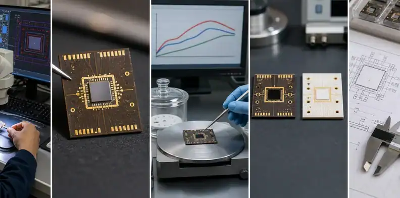
Quick Answer: BT substrate for MEMS sensor packaging is used when a sensor package needs a thin organic carrier with stable dimensions, low moisture uptake, controlled CTE, and moderate cost. It fits many consumer and mobile MEMS packages, while ceramic remains better for extreme heat, high power, harsh media, or very low thermal resistance.
Key takeaways
- BT is a practical carrier for many mobile MEMS, optical, fingerprint, pressure, and inertial sensor packages.
- The real decision is not “BT or MEMS”; it is whether the package needs organic fine routing, thin form factor, moisture control, or ceramic-grade environmental margin.
- Low-CTE and low-shrinkage BT grades can help package flatness and long-term sensor stability, but the supplier must state the actual material family.
- A quote-ready sensor package should include package format, die size, attachment method, pad pitch, thickness target, finish, and environmental test expectations.
MEMS buyers often start with the sensor die and leave the substrate choice vague. That creates a weak RFQ because the substrate affects package thickness, wire-bond or flip-chip routing, moisture behavior, reflow stress, and warpage. This article focuses only on the substrate role. It does not explain MEMS device physics or sensing algorithms; it explains when a BT carrier is a sensible packaging choice and when the design should move toward ceramic or another substrate family. To place this decision beside related material, application, and sourcing questions, use the complete BT PCB resource as the hub page.
| MEMS package situation | BT fit | Buyer evidence to request |
|---|---|---|
| Mobile inertial or optical sensor | Strong candidate | Low-CTE material family and thickness target |
| Harsh media pressure device | Review carefully | Ceramic or sealed package comparison |
| Compact sensor plus ASIC | Often useful | Pad map, attachment method, and finish |
| Quote input | Why it matters for MEMS | Release owner |
|---|---|---|
| Cavity, port, or lid note | Protects mechanical sensing path | Package engineering |
| Moisture or humidity condition | Affects drift and package stress | Reliability owner |
| Flatness target | Protects die attach and module fit | Assembly engineering |
Table of Contents
- Is BT substrate used for MEMS sensors?
- Why MEMS packaging often favors BT
- Which MEMS devices can use BT carriers?
- How moisture and CTE affect sensor stability
- BT vs ceramic substrate for MEMS
- When a MEMS design should avoid BT
- What to send for a MEMS substrate quote
- How to compare MEMS BT quotes
Is BT substrate used for MEMS sensors?
Yes. BT substrate is used in MEMS-related packaging when the device needs a thin, dimensionally stable organic carrier rather than a simple FR-4 board or a high-cost ceramic base. Mitsubishi Gas Chemical lists MEMS, optical sensors, fingerprint devices, RF modules, memory, CSP, BGA, flip-chip package, SiP, and module applications for its low-CTE BT material families, which is a useful public signal that BT belongs in the package-substrate conversation rather than only in ordinary PCB fabrication.
That does not mean every MEMS device should automatically use BT. A barometric sensor in a phone, a small inertial module, or a compact optical sensor may care most about thickness, fine routing, moisture resistance, and cost. A pressure sensor exposed to aggressive media, a high-temperature automotive location, or a module with strong thermal loading may need ceramic, metal, glass, or a package-specific construction instead.
A buyer should first identify the package role. BT is not the sensing membrane, proof mass, optical window, or ASIC. It is the carrier that connects the MEMS die, control IC, passive parts, balls, lands, pads, or flex interface. Once that boundary is clear, the substrate discussion becomes practical: can the BT build carry the pitch, thickness, finish, and reliability requirement without creating warpage or moisture risk?
Decision signal: Use BT for MEMS when the substrate is a thin organic carrier for interconnect and package support, not when the substrate must act as a high-temperature or high-conductivity structural material.
Why MEMS packaging often favors BT
MEMS packaging favors BT because the material family gives a useful balance of dimensional stability, heat resistance, insulation, and process cost. Low-CTE BT laminate and prepreg grades are built for IC plastic packages, with MGC describing low CTE, low shrinkage, heat resistance after moisture absorption, and coreless suitability in its public material lineup. Those features map well to sensor packages where small movements, moisture swelling, or reflow stress can change assembly behavior.
The most common purchasing mistake is treating a MEMS substrate as a miniature FR-4 PCB. The package carrier may need much tighter pad registration, cleaner surface finish control, thinner construction, and better flatness than a normal board. A BT substrate can sit between commodity PCB and ceramic: more package-friendly than standard FR-4, yet usually less specialized than alumina, AlN, LTCC, or glass ceramic routes.
BT also supports the manufacturing patterns that appear in small modules. Wire-bond pads, solder lands, flip-chip attach sites, microvias, and short signal paths can fit into a compact stack. When the sensor connects to an ASIC in the same module, the carrier must control routing density without turning the whole device into an expensive advanced interposer. That is where BT often earns a place.
Buyer call: Ask whether the supplier is quoting a package substrate process, not merely a small PCB made from a BT-labeled material.
Which MEMS devices can use BT carriers?
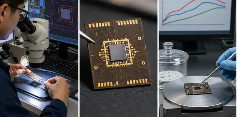
BT carriers can fit many consumer and mobile MEMS packages, including inertial sensors, microphones, pressure sensors, optical sensing modules, and biometric sensor assemblies. The better description is not a fixed device list; it is a package pattern. BT becomes relevant when the device uses a compact organic substrate to fan out the sensor die, ASIC, passives, shield, lid, or solder-ball interface.
Inertial modules can benefit from thin, stable packages because the product envelope is tight and the package is often assembled near other mobile components. Microphones and pressure sensors may use a different cavity or port structure, so the substrate decision has to include mechanical openings, lid attachment, cleanliness, and any acoustic or media path. Optical MEMS or proximity modules may add surface-finish, flatness, and assembly-height concerns.
Fingerprint and other biometric sensors deserve their own treatment because the sensing surface, module thinness, and wear environment create a narrower decision set. For that slice, see BT for fingerprint sensors. For broad material background, the BT fundamentals article explains the resin family and basic property trade-offs.
A practical RFQ should avoid vague labels such as “MEMS board.” State whether the substrate carries a bare die, packaged sensor, ASIC, lid, shield, cap, or connector. Also state whether the build is wire-bond, flip-chip, soldered module, or mixed assembly. Those details decide whether BT is simply possible or actually quote-ready.
Package rule: The device name matters less than the attachment method, pad pitch, thickness envelope, and environmental exposure.
How moisture and CTE affect sensor stability
Moisture and CTE matter because a MEMS package often measures small physical changes. Substrate swelling, die stress, package bow, or lid movement can shift calibration, weaken solder joints, or disturb a mechanical reference. BT does not remove those risks, but low-moisture and low-CTE grades reduce the amount of movement the package has to absorb.
A buyer should not quote only a headline property such as “low moisture.” Ask for the supplier’s material datasheet, laminate/prepreg family, storage condition, reflow assumption, and whether the material is a low-CTE package grade. MGC’s low-CTE BT material page is useful because it ties low shrinkage and low CTE to warpage reduction for IC packages. The supplier’s actual quoted grade still has to match the design.
CTE mismatch becomes visible during reflow and later thermal cycling. A MEMS die, ASIC, copper pattern, mold compound, lid, and organic substrate all move differently with temperature. Thin packages amplify that effect because there is less stiffness to resist bending. Good package design uses material choice, copper balance, die placement, and cure profile together, not as separate afterthoughts.
Stability check: Treat moisture and CTE as package-motion controls, not as generic datasheet decoration.
BT vs ceramic substrate for MEMS
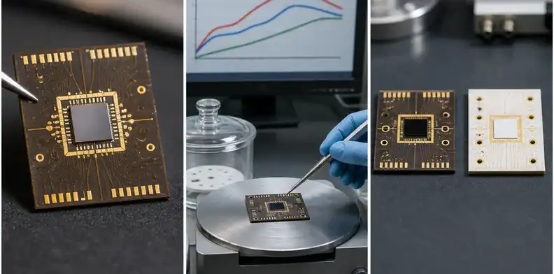
BT is usually the better starting point when the MEMS package is small, cost-sensitive, organic, and moderate in temperature. Ceramic is the safer starting point when the device sees high heat, aggressive media, high insulation stress, strong thermal paths, or a customer requirement that already names alumina, AlN, LTCC, or another ceramic route.
The comparison should not be reduced to one thermal number. Ceramic can provide higher stiffness, better high-temperature behavior, and stronger environmental margin, but it may raise cost, change metallization, limit some routing options, and affect assembly flow. BT gives organic package routing, thinner stack possibilities, and a familiar substrate process, but it must be controlled for moisture, flatness, and reflow stress.
For a deeper material comparison, use BT PCB vs ceramic PCB and the QueenEMS ceramic substrate options hub. The MEMS decision should come back to the package environment: consumer sensor, automotive under-hood position, medical instrument, industrial field module, or high-temperature measurement device.
A buyer can ask the supplier for two quote paths only when the files support both. If the die attach, land pattern, cavity, or lid construction is built around one material family, a second material quote may be misleading. In that case, ask first for a substrate feasibility review instead of a price comparison.
Material boundary: Choose BT for compact organic interconnect; choose ceramic when the substrate must carry harsh-environment or high-thermal responsibility.
When a MEMS design should avoid BT
A MEMS design should avoid BT when the operating condition pushes beyond what an organic package substrate should safely own. Examples include sustained high temperature, strong heat flow, aggressive fluids, high-voltage isolation, severe hermeticity needs, or a package drawing that already assumes ceramic thickness, metallization, or cavity geometry.
Another warning sign is unsupported fine geometry. BT can support fine-pitch package work, but the achievable line/space, microvia size, and yield depend on the supplier’s process and the material reinforcement. For finer routing limits, read BT fine-pitch capabilities. A sensor package that needs extremely fine redistribution may belong in ABF, silicon, glass, or another advanced substrate route rather than standard BT.
Flatness is also a stop point. A thin BT carrier with asymmetric copper, a large die, and a tight coplanarity rule may look feasible in a drawing but fail during reflow. In that situation, the buyer should request a warpage review before releasing tooling. The answer may be a different stack, a low-CTE grade, a changed copper balance, or a different substrate family.
Stop rule: Do not force BT into a MEMS package when temperature, media exposure, ultra-fine routing, or coplanarity risk is the dominant requirement.
What to send for a MEMS substrate quote
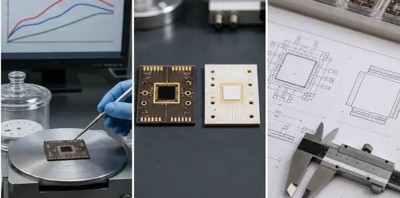
A useful MEMS substrate RFQ should include the substrate drawing, Gerber or ODB++ data, stack-up target, die size, pad map, bond or bump method, package height limit, finish, cleanliness notes, cavity or port requirements, and the expected reliability tests. If the package includes assembly, add the BOM, lid or cap material, adhesive or die attach preference, and inspection method.
The supplier should return more than a price. A strong reply states the BT material family, whether an equivalent grade is being proposed, the finish, line/space assumption, via structure, thickness tolerance, flatness or warpage check, and any feature that needs engineering approval. That is the difference between a substrate quote and a vague “small board” price.
Keep those sensor-package inputs under one revision so material choice, die attach, finish, and environmental exposure are reviewed together before the substrate route is priced.
Extra buyer notes for MEMS package release
MEMS packages often combine mechanical, electrical, and environmental requirements in one small outline. That makes the drawing more important than the material name. A package drawing should show ports, cavities, keepouts, lid areas, exposed pads, die attach areas, and any surfaces that must stay clean. If those features are missing, the supplier may quote the copper pattern but miss the feature that actually protects sensor performance.
Another useful check is assembly ownership. Some suppliers quote only the bare BT substrate. Others may quote substrate plus die attach, wire bonding, lid placement, SMT, or module assembly. The quotation should state the handoff point clearly. For example, a bare substrate quote should not be expected to prove acoustic response or calibration drift; an assembled module quote needs a broader evidence package.
For overseas buyers, documentation matters because the sensor package may move from prototype to pilot quickly. Keep material approval, stack-up, finish, and environmental assumptions attached to the RFQ. That record lets engineering decide whether a repeat order can use the same BT route or whether a changed sensor die, lid, or adhesive requires a new substrate review.
How to compare MEMS BT quotes
Compare MEMS BT quotes by package role, material family, finish, flatness evidence, and assembly ownership. A supplier that names those assumptions is giving a stronger answer than a supplier that only confirms the word BT.
Use the QueenEMS contact page to share the MEMS package drawing, substrate files, die interface, thickness envelope, finish target, environmental test expectation, and quantity stages. The review can decide whether BT sensor substrate support is a practical organic-carrier route or whether ceramic, HDI, or another substrate family deserves the first quote.
FAQ
Is BT used for MEMS sensors?
Yes. BT is used as an organic carrier in many MEMS-related package formats, especially when thin construction, fine routing, and moderate cost matter.
Why choose BT for MEMS packaging?
Choose BT when the package needs better dimensional stability and package-substrate behavior than ordinary FR-4 while staying in an organic manufacturing route.
Is ceramic better than BT for MEMS?
Ceramic is better for harsh heat, media, isolation, or thermal needs. BT is usually more practical for compact consumer and mobile sensor packages.
What files are needed for a MEMS BT quote?
Send substrate data, package drawing, die or pad map, attachment method, finish, thickness target, reliability tests, and quantity stages.
Sources
- Mitsubishi Gas Chemical, Low-CTE BT resin laminate lineup
- Global Electronics Association, IPC-6921 organic IC substrate standard
Written by the QueenEMS Engineering Team
Upload your files today · Free DFM check before production · Ship worldwide
Get your PCB prototypes in as fast as 24 hours. We handle FR4, Rogers, and Flex up to 60 layers — free prototypes for 2–4 layer boards, no minimum order.
Just upload your Gerber + BOM — we source every part, assemble, and inspect (AOI + X‑Ray) so you don't have to chase suppliers. Boards ship in as fast as 24 hours.