
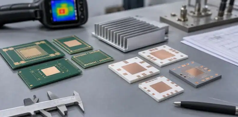
Quick Answer: Compare the actual BT laminate grade and ceramic construction against the package, routing, insulation and heat-path requirements. Ceramic can reduce resistance through an insulating heat path; BT can support dense organic package structures and other paths for heat removal. Neither material family has one universal cost, CTE, dielectric value or power limit.
The ceramic PCB overview distinguishes a finished circuit from a bare substrate, a useful starting point for this BT comparison.
Key takeaways
- Named ceramic products can have much higher bulk conductivity than a BT grade; this does not predict the same improvement in module temperature.
- BT can still win when signal integrity, cost, weight, and package-substrate maturity matter more than heat spreading.
- Ceramic is not automatically better; using it for a moderate-heat package can add cost, brittleness, and sourcing complexity.
- Start from the heat path and reliability requirement, then choose the substrate family.
Table of Contents
- BT vs ceramic PCB: which should you choose?
- How big is the thermal conductivity gap?
- Why higher thermal conductivity is not always the answer
- Where BT fits: package structure and electrical requirements
- Where ceramic fits: insulated heat paths and attachment
- How do the two compare on cost?
- When does your design actually need ceramic?
- What to Verify Before Choosing the Substrate
BT vs ceramic PCB: which should you choose?
Consider ceramic when a thermally conductive electrical insulator is needed beneath a die, LED or power device. Consider BT when the package requires an organic multilayer substrate and its complete heat path meets the temperature target. MGC documents BT use in IC packages and chip-LED substrates, so neither “LED” nor “power electronics” alone determines the material.
The decision is not ‘higher thermal conductivity always wins.’ A substrate with too much cost, brittleness, or process mismatch can be the wrong solution for a moderate thermal load.
In a ceramic comparison, the first question is the size of the heat-path problem. BT remains an organic laminate, so it can help with package stability and higher-performance routing without behaving like alumina or AlN. A design that needs bulk heat spreading, dielectric isolation under high power, or direct thermal conduction should be screened differently from a compact BT module.
A better material decision starts with the thermal model. If the board only needs an organic substrate with better package behavior, BT may remain sensible; if the heat must leave through the dielectric, ceramic belongs in the comparison.
First identify the thermal bottleneck. Heat may leave through a dielectric, copper planes, vias, package lid or chassis. A limitation in the dielectric is a reason to compare thermal constructions, including ceramic, but not proof that only ceramic will work. For related organic-substrate topics, see the BT PCB overview.
How big is the thermal conductivity gap?
The following are published product examples, not family-wide limits. MGC’s HL832NS BT data and Rogers’ curamik Thermal AlN data report different conditions. The comparison identifies questions to resolve; it is not a controlled head-to-head test.
| Property | MGC HL832NS BT | Rogers curamik Thermal AlN |
|---|---|---|
| Thermal conductivity | 0.6 W/mK, typical; direction and temperature not specified in the public table | 170 W/mK at 20 °C |
| Linear CTE | 10 ppm/°C in X/Y, α1 entry; temperature interval not stated in the public table | 4.8 ppm/K over 20–300 °C for the ceramic |
| Electrical data needed for routing | Dk 4.4 and Df 0.006 at 1 GHz in the MGC table | Obtain values and method for the selected grade, frequency and conductor geometry |
Before using these numbers in a design model, obtain comparable thermal-conductivity direction, temperature and measurement conditions. Also distinguish the ceramic alone from a copper-clad substrate. The missing MGC test conditions are a limitation, not permission to assume room-temperature through-plane performance. Neither table establishes a finished board’s cost or power rating.
The evidence package should separate electrical substrate needs from heat-transfer needs. BT data should cover laminate and routing assumptions; ceramic data should cover substrate material, metallization, isolation, and thermal path.
Evidence for this choice should prove the heat path. BT proof is usually about laminate behavior, routing, copper, via strategy, and assembly flow. Ceramic proof is about substrate material, metallization, copper bonding or plating route, isolation, flatness, and thermal-cycle reliability. A quote that does not name the heat source is not comparable.
A low-cost quote is not useful if it ignores the heat path. Ask whether the proposed material actually meets the thermal function before comparing price.
Why higher thermal conductivity is not always the answer
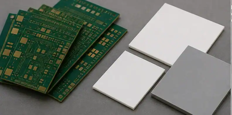
Higher thermal conductivity helps only when the substrate is part of the limiting heat path. If the actual bottleneck is package interface, die attach, air flow, heat sink contact, or enclosure design, changing BT to ceramic may not solve the problem.
Draw the heat path from the die through attachment, copper, substrate, interfaces and cooler. Assign the allowed temperature rise to the complete path before deciding how much a substrate change can help.
A Slab Calculation Shows Why Conductivity Is Not the Whole Gain
For a uniform slab with one-dimensional steady heat flow, thermal resistance is R = t/(kA): thickness t in metres divided by conductivity k in W/mK and area A in square metres. This model excludes spreading, vias, copper layers, contact resistance and temperature dependence. It is a screening calculation, not a module simulation.
Assume, solely for an illustrative calculation, a BT layer 0.10 mm thick with k = 0.6 W/mK and an AlN layer 0.63 mm thick with k = 170 W/mK. Assume the same conducting area of 100 mm², constant properties and no lateral heat flow. The conductivity inputs resemble the product examples above, but their measurement conditions are not matched; the calculation is not a verified comparison of those products.
| Assumed slab | Calculation | Slab resistance |
|---|---|---|
| BT | 0.00010 / (0.6 × 0.00010) | 1.67 K/W |
| AlN | 0.00063 / (170 × 0.00010) | 0.037 K/W |
Now assume all other parts of each heat path contribute the same 3.0 K/W in series. The totals become about 4.67 K/W and 3.04 K/W. Under a further assumed steady dissipation of 5 W, the model gives temperature rises of about 23.3 K and 15.2 K. These are calculated values from the stated assumptions, not measured board temperatures or promised savings.
The exercise identifies the next measurement: determine whether the shared interface and cooler resistance is actually dominant. In a real design, changing substrates can also change attachment, area and heat spreading, so those terms cannot simply be held constant without evidence. Use a representative assembly measurement or validated thermal model to replace the assumptions before releasing the material change.
Thermal conductivity describes heat conduction in both material systems. Tg describes an organic laminate’s glass transition and is a different property; Dk describes electrical response. A high Tg does not mean high thermal conductivity, and a high conductivity does not establish allowable assembly temperature.
The heat path should be drawn before the material is chosen. Start at the junction or die, then follow solder, copper, dielectric, base material, interface material, heat sink, and ambient. If most of the temperature rise sits in the interface or enclosure, ceramic may not fix the product. If the dielectric layer under the device is the bottleneck, BT will not behave like AlN or alumina no matter how attractive the price is.
Parameter review should begin with power density and junction target. Ceramic conductivity matters only if the substrate carries heat away from the device; BT can still be correct when heat leaves through copper planes, chassis contact, or the component package. Ask suppliers to show which part of the thermal path their substrate is solving.
Where BT fits: package structure and electrical requirements
BT can fit an organic package process where layer structure, routing, warpage control and assembly compatibility matter. Electrical properties vary by grade and frequency: the MGC examples above do not support a universal Dk of 4.0 or a blanket loss advantage over FR-4. Compare the actual laminate and circuit geometry.
For compact package substrates, this balance may matter more than raw thermal conductivity. A memory package, RF module, or consumer package may not benefit from ceramic if the heat load is moderate.
Thermal trade-offs often appear after the first layout review. A supplier may quote BT because the routing is compact, while the thermal engineer expects a ceramic path under the power device; that mismatch should be resolved before prototype spend.
A useful thermal note states whether the board must spread heat through the substrate or only survive assembly and package stress. That single distinction often decides whether BT or ceramic belongs in the quote.
Where ceramic fits: insulated heat paths and attachment
Ceramic is a candidate when the design needs an electrically insulating heat path and a compatible thermomechanical structure. CTE matching depends on the actual materials, copper, attachment and temperature range. MGC also offers low-CTE BT grades; “ceramic” alone does not guarantee the best match or the least package warpage.
For the ceramic branch, use QueenEMS ceramic PCB manufacturing and the article on when the ceramic cost premium pays off.
The ceramic branch also changes the manufacturing conversation. Instead of only laminate, drill, plating, and solder-mask questions, the buyer may need to review substrate flatness, copper bonding method, metallization, cracking risk, isolation spacing, and die-attach compatibility. Those controls can be worth the cost in power modules or laser packages, but they add unnecessary complexity when the board only needs moderate heat tolerance.
If a proposed substitution changes layer structure, routing density or die attachment, price the resulting assembly as well as the substrate. A nominal material saving can be offset by extra interconnection, tooling or verification work.
The cost trade-off should start with the thermal bottleneck. BT can save money when heat leaves through copper, chassis, or airflow and the substrate mainly provides package stability. Ceramic earns its premium when the insulating substrate itself has to carry heat away from the device.
How do the two compare on cost?
Obtain quotes for manufacturable constructions that meet the same requirements. An organic package substrate and a metallized ceramic can have different layer counts, features, fixtures and assembly scope. Their material names alone do not establish which finished solution costs less.
Cost comparison should still be application-specific. If ceramic prevents thermal failure, the premium may be justified. If BT meets the temperature and reliability target, ceramic may only add complexity.
The cost curve also changes with volume. A prototype ceramic build can feel disproportionately expensive because tooling, setup, metallization checks, and supplier review are spread across very few pieces. A BT prototype may be easier to absorb when the design sits inside familiar organic fabrication rules. For production, the comparison should include yield, inspection, assembly handling, and failure cost, not only bare-board price.
The approval boundary should follow the heat path. Thermal or power engineering owns the BT-versus-ceramic choice, purchasing compares complete material routes, and quality checks certificates and inspection evidence.
The risk in the BT-versus-ceramic decision is that the lower-cost organic route may be chosen before the heat path is proven. If ceramic was required for thermal conduction or isolation, engineering has to approve any return to BT with a thermal argument.
When does your design actually need ceramic?
Consider a change when analysis or representative tests show that the present construction cannot meet a defined temperature, insulation, package or reliability requirement. Verify that the proposed ceramic route fixes the limiting path without creating an unacceptable routing, attachment or mechanical constraint.
A poor thermal quote names BT or ceramic before it names the heat source, power level, junction limit, and interface path. That order is backwards. The supplier response should show where temperature rise is expected and why the proposed substrate can handle that section of the path.
Before choosing on cost, send the thermal target, insulation need, copper or metallization assumptions, and assembly process. The supplier response should say which material route can meet them.
What to Verify Before Choosing the Substrate
Verify the same four items for each candidate: the thermal path, electrical construction, attachment scheme and available fabrication route. Then compare representative first-build evidence and the complete quotation. A material property can help select a candidate; it cannot release the product by itself.
For borderline cases, compare the real temperature rise and reliability target before changing the substrate family.
The buyer should also ask how the supplier will verify the first build. For BT, that may mean stackup confirmation, impedance coupons, dimensional checks, and assembly review. For ceramic, it may mean substrate thickness, copper adhesion, flatness, metallization quality, and packaging protection. These are different evidence packages. Put the acceptance evidence into the quote request so a lower price does not remove the inspection step that proves the chosen material path is working.
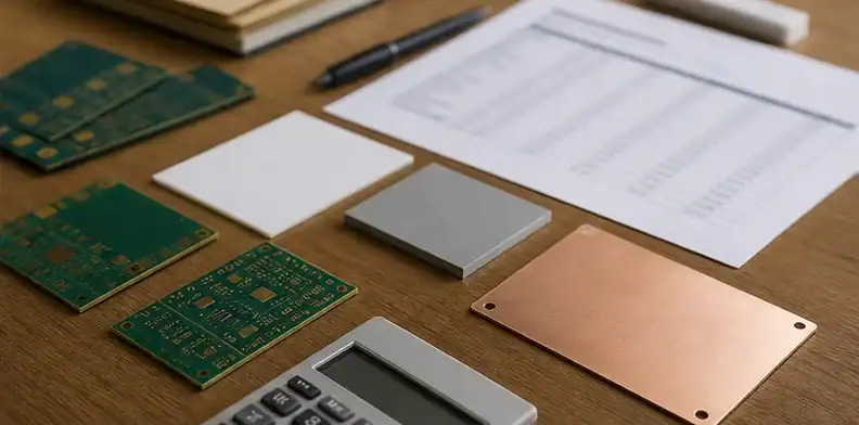
Check whether the quoted process supports the required multilayer routing, vias, die attach, wire bonding or soldering. A package substrate is not automatically transferable to a general PCB line, and a ceramic substrate is not automatically difficult to assemble. Ask which drawing, test and process changes follow from the proposed construction.
FAQ
Is ceramic always better than BT?
No. Compare actual grades and complete constructions. Ceramic can help an insulating heat path, while BT can fit organic package routing and assembly requirements. The result depends on the design and its evidence.
When do I need ceramic?
Consider ceramic when its construction addresses a verified thermal, electrical or mechanical limit in the design. Confirm the complete heat path, routing and attachment before replacing the current substrate.
Is ceramic more expensive?
Not necessarily. Compare quotes for the required layer structure, metallization, geometry, assembly and evidence at the same quantity. This article does not provide market prices for a specific build.
Can BT handle power electronics?
A material family alone does not set a board’s power limit. BT can be part of a power-electronics construction when heat removal, insulation, interconnections and reliability requirements are met. High device power does not prove all of that heat must pass through the laminate.
Send QueenEMS a BT versus ceramic substrate question
Share the heat source, wattage, junction or case target, package outline, available board area, stackup, quantity, and cost ceiling through QueenEMS contact. QueenEMS can review whether a BT organic substrate option is enough or whether alumina, AlN, or another ceramic route should be quoted.
Sources
Written by the QueenEMS Engineering Team
Upload your files today · Free DFM check before production · Ship worldwide
Get your PCB prototypes in as fast as 24 hours. We handle FR4, Rogers, and Flex up to 60 layers — free prototypes for 2–4 layer boards, no minimum order.
Just upload your Gerber + BOM — we source every part, assemble, and inspect (AOI + X‑Ray) so you don't have to chase suppliers. Boards ship in as fast as 24 hours.