
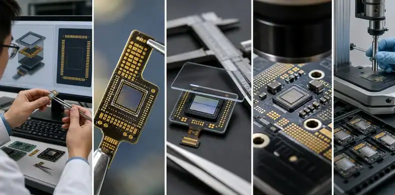
Quick Answer: BT PCB for fingerprint sensor and biometrics is a good fit when the module needs a thin package carrier, stable dimensions, low moisture uptake, fine routing, and cost control for consumer-scale production. It is not about the biometric algorithm; it is about the substrate that lets the sensor die, ASIC, pads, shield, and external interface fit inside a small reliable module.
Key takeaways
- Fingerprint and biometric modules often use thin organic carriers, and BT is one practical material family for that role.
- Under-display, wearable, and compact modules care about thickness, flatness, moisture, pad registration, and surface finish before broad material labels.
- Coreless or very thin BT options can help package height, but warpage and handling risk must be reviewed early.
- The RFQ should describe sensing surface constraints, module height, die attachment, finish, pad pitch, and reliability exposure.
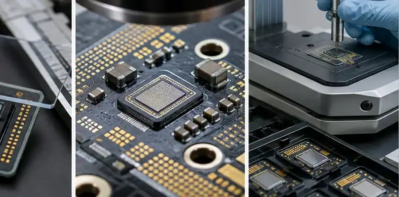
A fingerprint module looks simple from the outside, but the substrate decision is not simple. The carrier may support the sensing die, companion IC, lands, shielding, flex connection, BGA pads, or a molded package. A weak request such as “quote BT board for fingerprint” leaves the supplier guessing about thickness, finish, coplanarity, and reliability tests. This article narrows the discussion to the biometric package substrate and links back to the broader BT for MEMS sensor packaging page for general sensor context. For adjacent questions on specifications, package use cases, cost, and supplier review, the BT PCB knowledge hub gives the broader context.
| Biometric module type | BT review focus | Quote evidence |
|---|---|---|
| Under-display module | Height and flatness | Section view and finished thickness |
| Wearable sensor | Moisture and handling | Storage, finish, and seal assumptions |
| Access-control reader | Repeatability | Material revision and inspection plan |
| Pad function | Likely finish path | Approval check |
|---|---|---|
| Wire-bond finger | ENEPIG baseline | Bonding owner confirmation |
| Solder-only land | ENIG or approved option | Assembly acceptance |
| Test or contact pad | Case-specific | Contact wear or probe requirement |
Table of Contents
- Is BT used for fingerprint sensor packaging?
- Why biometric modules favor thin BT substrates
- How thin can the BT carrier go?
- BT for under-display and wearable sensors
- How BT supports CSP miniaturization
- Reliability risks in biometric modules
- What to send for a biometric BT quote
- How to compare biometric BT quotes
Is BT used for fingerprint sensor packaging?
Yes. BT is used in fingerprint and biometric sensor package contexts when the product needs a compact organic substrate with controlled thickness, dimensional stability, and fine interconnect. MGC’s public low-CTE BT material information lists fingerprint and optical sensor packages, plus MEMS, CSP, BGA, flip-chip, SiP, and module uses, which supports the basic point that BT is a real package-substrate option for this category. The buyer still has to define whether the product is capacitive, optical, ultrasonic, wearable, or access-control hardware, because each format changes the module stack. Decision signal: Treat BT as a package carrier choice for biometric hardware, not as the sensing technology itself.
Why biometric modules favor thin BT substrates
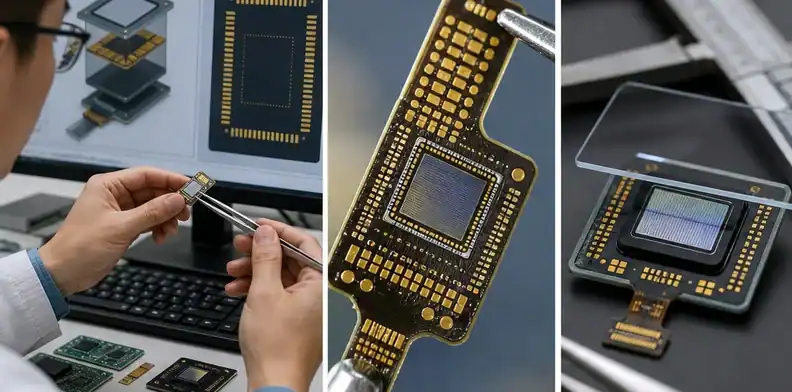
Biometric modules favor thin BT substrates because the product envelope is tight. Phones, locks, wearables, handheld instruments, and compact access devices often leave little vertical room for the sensor package. A BT build can offer a thinner, more package-oriented carrier than ordinary FR-4 while keeping an organic manufacturing route that is practical for quantity production. Thinness only helps when the package stays flat, so the supplier should discuss warpage and handling before the buyer approves a thinner core or coreless route. Package rule: A thin biometric substrate is valuable only when flatness, finish, and moisture exposure are controlled.
How thin can the BT carrier go?
The practical BT carrier thickness depends on the material grade, core or coreless construction, copper distribution, layer count, routing density, and handling method. Public MGC material tables list thin copper-clad laminate and prepreg options for low-CTE BT families, including very thin prepregs and 30 micrometer class CCL entries in some package material lines. Those entries are material availability signals, not automatic manufacturing promises. For a deeper thickness framework, see choosing BT thickness. Thickness check: Do not approve a thinner BT carrier until handling, warpage, and assembly-height stack are checked together.
BT for under-display and wearable sensors
Under-display and wearable sensors increase the pressure on substrate thickness and package consistency. The module may sit near optical layers, flexible circuits, shielding, adhesives, coatings, or a curved enclosure. A small change in carrier flatness or height can become a product-level fit problem rather than only a PCB tolerance issue. Wearable products bring sweat, cleaning, movement, and repeated temperature changes, so substrate review should be tied to sealing and reliability planning. Use-case call: Under-display and wearable work should quote the full module height and exposure condition, not only the BT laminate name.
How BT supports CSP miniaturization
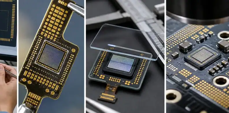
BT supports CSP miniaturization by giving the package designer a thin organic platform for dense pads, short routing, and compact die-to-board transition. Fingerprint and biometric modules often live in consumer electronics where the package must be small enough for the enclosure while still being manufacturable at scale. Fine-pitch work is not free; the achievable line and space, microvia size, and pad registration depend on the supplier’s process. For adjacent package design context, see QueenEMS’ small package design and CSP and BGA assembly pages. Miniaturization rule: BT can support compact CSP-style biometric packages, but the finish and fine-routing class must match the actual attach method.
Reliability risks in biometric modules
The main reliability risks are moisture exposure, reflow stress, handling damage, flatness loss, surface finish mismatch, and unclear acceptance criteria. A biometric module may be small, but it still sees mechanical pressure, human-contact environments, cleaning cycles, and assembly heat. Ask for the acceptance class, finish inspection, warpage or coplanarity check, material datasheet revision, and any environmental test linked to the end product. Acceptance rule: A biometric BT quote should define substrate evidence, while sensor performance and product sealing stay with the module design owner.
What to send for a biometric BT quote
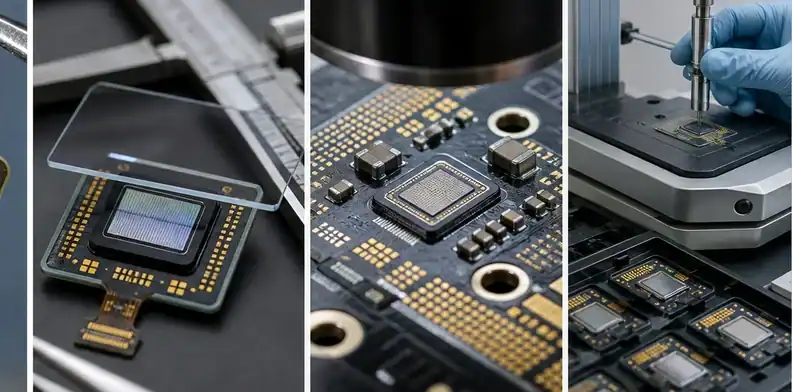
Send Gerber or ODB++ data, stack-up, package drawing, module height limit, die size, pad pitch, bond or bump method, surface finish, shield or cover clearance, environmental exposure, quantity stages, and inspection expectations. If assembly is included, add BOM, CPL, adhesive preference, stencil or solder-ball notes, and test flow. Keep the biometric module inputs tied to the same revision so carrier thickness, sensing surface clearance, finish, and assembly ownership are not quoted as separate assumptions.
Extra buyer notes for biometric package release
Biometric packages usually fail quietly before they fail visibly. A carrier that is slightly bowed can still pass a quick visual inspection, yet the finished module may show poor contact, uneven adhesive thickness, weak solder joints, or inconsistent sensor-to-cover spacing. That is why the RFQ should include the final module height and the stack above the sensor, not only the BT substrate thickness.
The sensing surface also changes the substrate review. A capacitive sensor may care about electrode geometry and dielectric spacing. An optical module may care more about mechanical height, cleanliness, and alignment. An ultrasonic or wearable format may add sealing and pressure concerns. The supplier does not need to know the algorithm, but it does need enough mechanical and assembly context to avoid quoting the wrong carrier.
Ask for finish evidence early. A solder-only biometric module can often be priced around ENIG or another solderable finish. A design with wire bonding should start from ENEPIG or a validated bondable finish. If the RFQ does not mark which pads are bonded and which pads are soldered, a supplier may choose a cheaper finish that makes the package hard to assemble.
Small pilot quantities deserve the same substrate definition as production. The pilot lot may be only a few panels, but it creates the reference for the scale-up build. Record material family, thickness, finish, flatness target, and any approved alternate before the first article is accepted. That keeps a successful sample from becoming a fragile one-off.
For under-display programs, the substrate review should include what sits above and below the BT carrier. Cover glass, optical adhesive, flex tail, shield can, elastomer, or enclosure ribs can all set a tighter height window than the bare substrate drawing shows. A quote that ignores those surrounding parts may pass fabrication and still fail module integration.
The inspection plan should match how the module fails. If the risk is solder coplanarity, ask for flatness or warpage evidence. If the risk is wire bonding, ask for bondable finish evidence and cleanliness controls. If the risk is module height, ask how thickness is measured and whether the number is finished substrate, assembled substrate, or complete module.
Biometric projects also need clean revision control because sensor vendors may change die pad maps, cover material, or ASIC pairing during development. A small die change can alter copper balance, pad pitch, or assembly heat exposure. When the design changes, do not assume the previous BT quote remains valid; ask for a focused delta review instead.
For overseas sourcing, the most useful supplier answer is a short engineering note that names the carrier route. It should say whether the supplier is quoting a core BT substrate, coreless BT carrier, HDI-like board, or assembled module. That single distinction prevents purchasing from comparing unlike quotes and helps engineering decide what evidence is missing.
Typical biometric substrate scenarios
A phone-side fingerprint module usually puts the harshest pressure on height and pad density. The substrate may need to fit beside a flex tail, shield, adhesive stack, and cover layer. In that case, the buyer should send a mechanical section view, not only the copper data. The section view tells the supplier whether the BT carrier is being judged by finished thickness, coplanarity, or only electrical routing.
A wearable biometric sensor may look similar in size but faces a different environment. Sweat, cleaning, repeated bending of the housing, and body-temperature cycling can create reliability issues that do not appear in a phone prototype. The RFQ should say whether the substrate sits inside a sealed module or near the product boundary. That detail affects finish, storage, and environmental evidence.
An access-control fingerprint module often has more room than a phone, but it may face outdoor humidity, user pressure, and longer service expectations. Here the substrate decision may be less about extreme thinness and more about stable supply, documented finish, and repeatability. A slightly thicker BT carrier may be safer than a coreless option if height is not the limiting factor.
Supplier replies should be judged by whether they name the module assumption. A useful answer says, for example, that the design is being quoted as a solder-only BT carrier with ENIG and a defined thickness, or as a wire-bondable BT carrier with ENEPIG and flatness review. A weak answer only says that BT is available.
For the first quote round, ask for one recommended build and one optional risk-reduction change. The optional change might be a thicker carrier, different finish, relaxed pad spacing, or revised copper balance. That keeps the discussion practical and gives engineering a clear trade-off instead of a long list of generic warnings.
Quote review questions for biometric BT
Before comparing prices, ask whether the quote includes only the bare carrier or any assembly work. Many biometric projects mix substrate fabrication, die attach, bonding, shielding, flex attachment, and final module test. A low bare-substrate price may be irrelevant if the buyer actually needs an assembled sensing module.
Ask how the supplier will protect the finish before assembly. Biometric substrates are small, but their pads can be sensitive to contamination and storage. The supplier should explain packaging, labeling, and shelf-life assumptions, especially when parts will be shipped across borders before assembly.
Check whether the material alternate policy is realistic. If the drawing names one BT grade, the supplier may offer an equivalent to improve lead time. That can be fine, but engineering should compare CTE, thickness availability, moisture behavior, and finish compatibility before accepting the change.
For a clean first article, request one concise review note: confirmed BT route, finished thickness, finish, critical pad pitch, flatness assumption, and open risks. That note gives the design team a fast way to approve or reject the quote without digging through scattered email.
One final sourcing point: keep the biometric substrate quote separate from enclosure or cover-lens assumptions unless the same supplier owns module integration. This prevents a substrate supplier from being judged on optical stack performance while still making sure the substrate data is useful for the module assembler.
How to compare biometric BT quotes
Compare biometric BT quotes by carrier thickness, pad function, finish, module height, and whether the quote includes assembly. A low substrate price is not useful when the project actually needs a verified module stack.
For a biometric carrier review, send the pad map, module height limit, sensing-surface stack, finish requirement, assembly scope, and pilot quantity from the QueenEMS contact page. QueenEMS can check the BT biometric carrier review path against the package and flag whether substrate fabrication should be quoted separately from module assembly.
FAQ
Is BT used for fingerprint sensors?
Yes. BT is used as a package carrier for some fingerprint and biometric modules where thin organic construction and stable interconnect are needed.
Why does thin BT matter for biometrics?
It helps fit the sensor package into phones, wearables, and compact devices, but only when warpage and handling are controlled.
Is BT suitable for under-display sensors?
It can be suitable when the under-display module needs a thin organic carrier. The optical or acoustic stack still has to be reviewed separately.
What finish should a biometric BT substrate use?
Use ENEPIG or another validated bondable finish for wire bonding; ENIG may fit solder-only modules when the design owner approves it.
Sources
- Mitsubishi Gas Chemical, Low-CTE BT resin laminate lineup
- Global Electronics Association, IPC-6921 organic IC substrate standard
Written by the QueenEMS Engineering Team
Upload your files today · Free DFM check before production · Ship worldwide
Get your PCB prototypes in as fast as 24 hours. We handle FR4, Rogers, and Flex up to 60 layers — free prototypes for 2–4 layer boards, no minimum order.
Just upload your Gerber + BOM — we source every part, assemble, and inspect (AOI + X‑Ray) so you don't have to chase suppliers. Boards ship in as fast as 24 hours.