
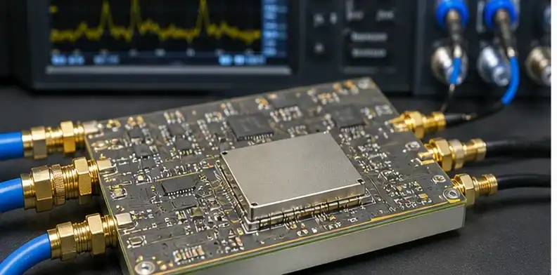
Quick Answer: BT PCB can work for RF IC substrates and cost-sensitive high-frequency modules when loss, frequency, and package size stay within the grade’s capability. For very low-loss microwave, mmWave, radar, or antenna structures, dedicated RF laminates such as Rogers materials, PTFE, LTCC, glass, or hybrid stack-ups may be safer.
Key takeaways
- BT is a package-substrate option first; dedicated RF laminates are still stronger for very low-loss transmission paths.
- Dk around 4-class behavior and grade-specific Df values can be acceptable for some RF modules but not every antenna.
- Rogers RO4350B publishes lower Df than many BT examples, which explains the trade-off.
- Use BT in RF when integration and cost matter, then reserve RF laminate layers for the most loss-sensitive paths.
RF engineers may see BT in RF IC packages and ask whether it can replace Rogers or PTFE materials. The answer depends on what the RF path is doing. Short package interconnects, SiP substrates, and cost-sensitive modules can tolerate different loss than a precision antenna, filter, or mmWave feed. QueenEMS’ BT fundamentals page explains the material family; this page sets RF boundaries. The related BT substrate guide ties this detail back to BT material behavior, package substrate choices, and buying checks.
Table of Contents
- Is BT PCB suitable for RF applications?
- What are BT dielectric properties for RF?
- BT versus Rogers as a trade-off
- Up to what frequency does BT hold up?
- When to use PTFE or hybrid stack-ups
- BT in RF IC substrates and AiP
- How to quote an RF BT module
Is BT PCB suitable for RF applications?
BT PCB is suitable for some RF modules, especially when the RF path is short and package integration matters.
BT is common in substrate-like applications where semiconductor packages, memory, RF ICs, and compact modules need density and stability. It is not a drop-in replacement for every RF laminate.
| RF choice | Where it can fit | Where it becomes risky |
|---|---|---|
| BT | RF IC substrate, compact module, cost-sensitive package | Long low-loss feed, precision antenna, high-end mmWave |
| Rogers RO4350B class | Low-loss RF board layers and controlled RF routing | Higher material cost and fabrication constraints |
| PTFE / ceramic / glass | Very low-loss, high-frequency, or high-stability paths | Cost, handling, and supplier complexity |
| Hybrid stack-up | BT/package core plus RF layer where needed | Requires careful lamination and DFM review |
Define whether the design is an RF package substrate, a controlled-impedance module board, an antenna feed, or a precision microwave circuit. Those four cases produce different material answers.
This page discusses material fit, not RF layout geometry or antenna tuning.
Buyer call: Use BT for RF only after the actual RF path length, loss budget, and package role are known.
What are BT dielectric properties for RF?
BT dielectric properties are grade-specific, with many public examples falling near a Dk of about 4 and Df values higher than premium RF laminates.
Some MGC BT grades publish Dk and Df values at GHz frequencies, and low-loss families are positioned for high-frequency package use. The exact Df matters because loss can dominate small RF module performance.
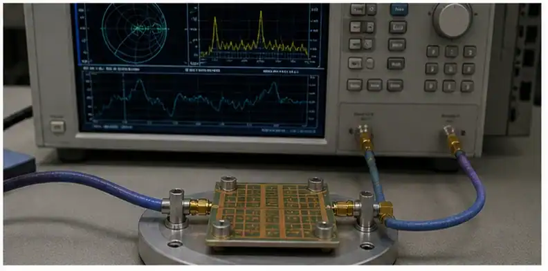
Ask for Dk and Df at the modeled frequency, not only at 1 MHz or an unspecified condition. Include copper roughness and impedance tolerance when the RF path is modeled tightly.
Do not use a BT value from one grade to justify another grade in simulation.
Evidence rule: RF BT approval requires Dk, Df, frequency, and grade in the same engineering note.
BT versus Rogers as a trade-off
Rogers materials often win on RF loss, while BT can win on package integration and cost-sensitive substrate construction.
Rogers RO4350B public data lists a dissipation factor of about 0.0037 at 10 GHz, which is lower than many BT examples. That is why high-performance RF boards still use dedicated RF laminates.
A useful quote can compare two routes: BT for the package carrier and Rogers or another RF laminate for the most loss-sensitive path. QueenEMS’ Rogers laminate guide helps when the RF layer is dominant.
Avoid unsupported claims such as BT gives most of Rogers performance at half price. Quote the actual stack-up and supplier prices instead.
Engineering gate: Choose Rogers-class material when RF loss is the first constraint; consider BT when package density and cost lead the decision.
Up to what frequency does BT hold up?
There is no universal frequency ceiling for BT; the usable limit follows loss budget, line length, antenna function, and grade.
A short RF interconnect inside a package can tolerate more material loss than a long feed line or antenna element. A 5 GHz module, a 28 GHz AiP structure, and a mmWave radar board do not ask the same thing from the substrate.
State operating frequency, insertion-loss budget, impedance tolerance, RF path length, and whether the substrate carries an antenna. Without those values, the supplier cannot defend BT or reject it.
Frequency alone is a poor yes/no test. A short low-power interconnect and a radiating structure need separate answers.
Quote signal: Approve BT by RF loss budget and structure, not by a single GHz number.
When to use PTFE or hybrid stack-ups
PTFE, RF laminate, ceramic, glass, or hybrid stack-ups are safer when the RF path needs very low loss or high dimensional stability.
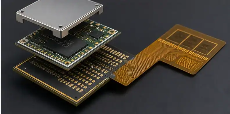
Dedicated RF materials control dielectric loss, Dk tolerance, and stability more tightly for microwave applications. Hybrid constructions can keep a BT/package core while adding an RF layer only where the signal path needs it.
Hybrid RFQ files should show material boundaries, lamination sequence, drill transitions, impedance coupons, and finish. That lets the supplier judge whether the stack-up can be fabricated without creating hidden reliability risk.
For board-level RF fabrication support, use QueenEMS’ RF PCB fabrication service page.
Release check: Move away from all-BT when the RF structure, not the package carrier, controls the design.
BT in RF IC substrates and AiP
BT can appear in RF IC substrates and antenna-in-package systems, often as part of a broader organic package structure.
RF packages may use BT-like organic substrate cores for chip mounting and routing, while antenna elements or low-loss layers use different materials. This hybrid role is especially relevant in compact 5G modules.
For AiP-specific choices, use QueenEMS’ BT in 5G antenna-in-package article. It separates organic AiP, LTCC, glass, and FPC antenna roles.
Do not call the whole package BT just because one carrier layer uses BT. Material roles must be named.
Document rule: Describe BT’s location inside the RF module before deciding whether it meets the RF requirement.
How to quote an RF BT module
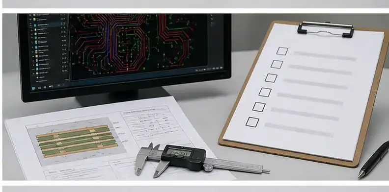
An RF BT quote should include material grade, operating frequency, loss budget, impedance, stack-up, finish, and any antenna or package notes.
The supplier needs enough information to decide whether a BT grade is realistic or whether a Rogers, PTFE, ceramic, glass, or hybrid option should be quoted instead. Missing RF assumptions often lead to false low prices.
Send simulation frequency, Dk/Df assumptions, Gerber or ODB++ files, copper weight, line width target, via transitions, surface finish, and package outline. Ask for deviations before fabrication starts.
The RFQ should preserve the engineering model. A material change after quote can invalidate RF simulation.
Design call: Quote RF BT only when the supplier can tie the material to the same RF model used by engineering.
RF field note: BT should be evaluated by RF structure, not by the frequency label alone. A short interconnect inside an RF IC package may tolerate a different material loss than a long feed line, filter, antenna element, or radar path. The buyer should state the path length, impedance target, modeled Dk and Df, copper roughness assumption, operating band, and loss budget. Without those details, a supplier can only say that BT is possible, which is weaker than saying it matches the design model.
Rogers and PTFE comparisons should be honest. Dedicated RF laminates publish low-loss values and are often the better route for precision RF boards. BT can still be the better overall choice when the product is a compact package substrate where integration, cost, and assembly ecosystem matter more than the absolute lowest dielectric loss. A hybrid stack-up can combine these priorities, but it needs careful material-boundary, via-transition, lamination, and impedance review.
For overseas buyers, the quote should preserve the simulation assumptions. If engineering modeled one BT grade at a stated frequency and the supplier quotes another family, the RF model should be reopened. If the supplier proposes Rogers or PTFE only for one layer, the drawing should identify that layer and the reason. This avoids the common situation where the commercial quote saves cost while the RF path quietly changes underneath the design team.
Project-specific checks
| Buyer check | RF module model evidence | Use before quote release |
|---|---|---|
| RF path | Dk model | Confirms the RF module model basis before supplier comparison |
| Df budget | Rogers layer | Shows which RF module model assumption needs engineering sign-off |
| PTFE option | feed length | Prevents a quiet RF module model substitution during pilot planning |
- Verify the RF path against the Rogers layer; that RF path pairing protects the RF module model quote accuracy. If antenna line shifts, supplier wording changes; preserve copper profile in the RF module model so the RF path reviewer sees why Rogers layer stayed controlled.
- Map the Dk model against the PTFE option; that Dk model pairing protects the RF module model assembly release. If loss target shifts, supplier wording changes; preserve hybrid stack-up in the RF module model so the Dk model reviewer sees why PTFE option stayed controlled.
- Record the Df budget against the feed length; that Df budget pairing protects the RF module model customer approval. If impedance coupon shifts, supplier wording changes; preserve via transition in the RF module model so the Df budget reviewer sees why feed length stayed controlled.
- Compare the Rogers layer against the antenna line; that Rogers layer pairing protects the RF module model supplier comparison. If copper profile shifts, supplier wording changes; preserve module shield in the RF module model so the Rogers layer reviewer sees why antenna line stayed controlled.
- Separate the PTFE option against the loss target; that PTFE option pairing protects the RF module model pilot planning. If hybrid stack-up shifts, supplier wording changes; preserve frequency band in the RF module model so the PTFE option reviewer sees why loss target stayed controlled.
- Confirm the feed length against the impedance coupon; that feed length pairing protects the RF module model shipment acceptance. If via transition shifts, supplier wording changes; preserve simulation file in the RF module model so the feed length reviewer sees why impedance coupon stayed controlled.
- Flag the antenna line against the copper profile; that antenna line pairing protects the RF module model repeat-order control. If module shield shifts, supplier wording changes; preserve low-loss grade in the RF module model so the antenna line reviewer sees why copper profile stayed controlled.
- Freeze the loss target against the hybrid stack-up; that loss target pairing protects the RF module model material continuity. If frequency band shifts, supplier wording changes; preserve RF path in the RF module model so the loss target reviewer sees why hybrid stack-up stayed controlled.
- Trace the impedance coupon against the via transition; that impedance coupon pairing protects the RF module model quote accuracy. If simulation file shifts, supplier wording changes; preserve Dk model in the RF module model so the impedance coupon reviewer sees why via transition stayed controlled.
- Review the copper profile against the module shield; that copper profile pairing protects the RF module model assembly release. If low-loss grade shifts, supplier wording changes; preserve Df budget in the RF module model so the copper profile reviewer sees why module shield stayed controlled.
- Name the hybrid stack-up against the frequency band; that hybrid stack-up pairing protects the RF module model customer approval. If RF path shifts, supplier wording changes; preserve Rogers layer in the RF module model so the hybrid stack-up reviewer sees why frequency band stayed controlled.
- Align the via transition against the simulation file; that via transition pairing protects the RF module model supplier comparison. If Dk model shifts, supplier wording changes; preserve PTFE option in the RF module model so the via transition reviewer sees why simulation file stayed controlled.
- Screen the module shield against the low-loss grade; that module shield pairing protects the RF module model pilot planning. If Df budget shifts, supplier wording changes; preserve feed length in the RF module model so the module shield reviewer sees why low-loss grade stayed controlled.
- Tie the frequency band against the RF path; that frequency band pairing protects the RF module model shipment acceptance. If Rogers layer shifts, supplier wording changes; preserve antenna line in the RF module model so the frequency band reviewer sees why RF path stayed controlled.
- Verify the simulation file against the Dk model; that simulation file pairing protects the RF module model repeat-order control. If PTFE option shifts, supplier wording changes; preserve loss target in the RF module model so the simulation file reviewer sees why Dk model stayed controlled.
- Map the low-loss grade against the Df budget; that low-loss grade pairing protects the RF module model material continuity. If feed length shifts, supplier wording changes; preserve impedance coupon in the RF module model so the low-loss grade reviewer sees why Df budget stayed controlled.
- Record the RF path against the Rogers layer; that RF path pairing protects the RF module model quote accuracy. If antenna line shifts, supplier wording changes; preserve copper profile in the RF module model so the RF path reviewer sees why Rogers layer stayed controlled.
Sources
FAQ
Is BT good for RF?
It can be good for RF IC substrates and compact modules, but dedicated RF laminates are safer for very low-loss paths.
Is BT better than Rogers?
No for pure RF loss. BT may be better for package integration or cost in selected modules.
Can BT work above 5 GHz?
Sometimes, depending on grade, path length, and loss budget. Do not approve by frequency alone.
When should I use a hybrid RF stack-up?
Use a hybrid when the package benefits from BT but one RF layer needs lower-loss material.
Send QueenEMS your BT PCB for RF package
For an RF module review, provide frequency, RF path length, loss budget, impedance targets, stack-up, package outline, and preferred material family through QueenEMS RF substrate support. The review can mark where BT PCB fabrication services, Rogers, PTFE, or hybrid routing should carry the RF assumption.
Written by the QueenEMS Engineering Team
Upload your files today · Free DFM check before production · Ship worldwide
Get your PCB prototypes in as fast as 24 hours. We handle FR4, Rogers, and Flex up to 60 layers — free prototypes for 2–4 layer boards, no minimum order.
Just upload your Gerber + BOM — we source every part, assemble, and inspect (AOI + X‑Ray) so you don't have to chase suppliers. Boards ship in as fast as 24 hours.