
Quick Answer: To accurately read ceramic PCB specifications, you must differentiate between theoretical material maximums and lot-specific tested values. Commercial AlN substrates typically deliver a real-world thermal conductivity of 150–180 W/m·K (not the theoretical 320 W/m·K), and safe production trace widths must be designed at 1.5 to 2 times the factory’s stated absolute minimum of 50 μm to avoid disastrous yield drops.
Key takeaways:
- Thermal conductivity on datasheets often lists pure material theoreticals; you need ASTM E1461 laser flash lot data.
- A factory stating “50 μm minimum trace width” means process limit, not production yield limit. Design at 100 μm for safety.
- Surface roughness (Ra) varies wildly by process: DPC hits < 0.5 μm, while Thick Film sits at 1–3 μm, impacting high-frequency RF loss.
- You cannot rely on theoretical dielectric breakdown voltage; demand IPC-6012 tested insulation resistance of ≥ 100 MΩ at 500V.
Table of Contents
- Why Do Ceramic PCB Datasheets Mislead Engineers More Than FR4 Specs?
- Spec #1: Thermal Conductivity — Why the Number on the Datasheet Is Often Theoretical?
- Spec #2: Copper Layer Thickness — How 0.1 mm vs 0.3 mm Changes Everything?
- Spec #3: Surface Roughness (Ra) — Why It Matters for RF and Soldering?
- Spec #4: Dielectric Breakdown Voltage — Theoretical vs Tested Values?
- Spec #5: Thermal Cycling Endurance — How Many Cycles and at What Temperature Range?
- Spec #6: Dimensional Tolerances — Warpage and Outline Tolerances After Sintering?
- Spec #7: Surface Finish Thickness — ENIG vs Silver Plating on Ceramic?
- Spec #8: Minimum Line Width and Spacing — Process Limit vs Production Yield Limit?
- What Are the Most Frequently Asked Questions About Ceramic PCB Specs?
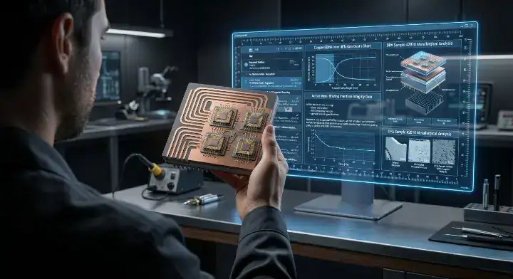
Do your thermal simulations perfectly match your prototype boards, or do the physical chips run surprisingly hot? When engineers migrate from FR4 to advanced ceramic substrates, they often take supplier datasheet numbers at face value, leading to severe thermal and yield miscalculations. At QueenEMS, we see this constantly, which is why we maintain a 99.7% first-pass yield rate by aggressively verifying lot-specific material data before production begins.
Why Do Ceramic PCB Datasheets Mislead Engineers More Than FR4 Specs?
The specifications for a ceramic PCB often mislead engineers because suppliers frequently publish raw, theoretical material properties (like an AlN thermal conductivity of 320 W/m·K) instead of the actual, post-processing performance data (which usually drops to 150–230 W/m·K). FR4 materials are highly standardized by IPC, meaning the data sheet closely matches the physical board. Ceramic boards, however, undergo extreme thermal sintering and metallization that fundamentally alter their final mechanical and thermal behaviors.
What causes the discrepancy? Different manufacturing processes completely change the final board capability. A DPC factory highlights copper uniformity, while a DBC factory focuses entirely on thermal cycling survival. You cannot use a generic checklist across different technologies. Before committing to a supplier, you must understand how to evaluate a ceramic PCB manufacturer to separate marketing numbers from production reality.
- FR4 Datasheets: Highly standardized, representing final board state.
- Ceramic Datasheets: Often represent raw, theoretical material maximums.
- The Solution: Demand lot-specific testing data for your exact production batch.
| Specification | What the Datasheet Says | What You Should Actually Ask |
|---|---|---|
| Thermal Conductivity | 230 W/m·K | What is the lot-specific ASTM E1461 test result? |
| Breakdown Voltage | 15 kV/mm | What is the IPC-6012 tested insulation resistance at 500V? |
| Min Trace Width | 50 μm | What is your Cpk value for a 50 μm trace in mass production? |
| Thermal Cycling | “Pass” | How many cycles at -40°C to +150°C, and what is the peel strength after? |
Demand lot-specific test certificates if you are designing a high-power module. Avoid relying on generic PDF marketing datasheets downloaded from a supplier’s main website.
Bottom line: Treat a generic ceramic datasheet as a theoretical marketing brochure; your engineering calculations require lot-specific test certificates.
Spec #1: Thermal Conductivity — Why the Number on the Datasheet Is Often Theoretical?
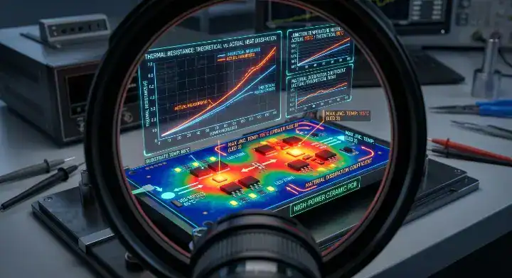
When evaluating ceramic PCB specifications, the thermal conductivity number listed is almost always a theoretical maximum; for instance, a datasheet might claim 230 W/m·K for AlN, while the actual commercial board tests at 150–180 W/m·K due to grain boundary impurities and sintering density variations. Al₂O₃ similarly claims a theoretical 20–24 W/m·K, but standard 96% purity boards usually measure around 20–22 W/m·K in reality.
Engineers on Reddit’s r/PrintedCircuitBoard frequently post: “The supplier claims AlN is 230 W/m·K, but my thermal simulation is way off. If I simulate with 150 W/m·K, it matches my physical test. Why?” We fix this exact error regularly. A power LED module client came to us with a thermal runaway problem. Their datasheet specified AlN at 200 W/m·K, but junction temperatures were running 35°C above simulation. According to Electronic Design (electronicdesign.com), using nominal rather than tested thermal data causes up to a 35% error in thermal margin calculations. We requested the actual material test certificates and found the AlN was only tested to 148 W/m·K. We helped the client revise their model, and the simulation instantly matched reality. They then sourced AlN with certified 170–180 W/m·K lot-specific data, and junction temperatures dropped 22°C. The supplier swap cost zero — we just demanded the correct ASTM E1461 test data.
- Al₂O₃ (96%): Theoretical 24 W/m·K vs Actual 20–22 W/m·K.
- AlN: Theoretical 320 W/m·K vs Commercial Actual 150–230 W/m·K.
- Testing Standard: Always verify using the ASTM E1461 laser flash method.
Bottom line: Never input a datasheet’s theoretical thermal conductivity into your simulation software; force the supplier to provide the ASTM E1461 laser flash measurement for your specific batch.
Spec #2: Copper Layer Thickness — How 0.1 mm vs 0.3 mm Changes Everything?
The copper layer thickness in ceramic PCB specifications radically alters both current-carrying capacity and mechanical stress, with DPC processes typically offering thin 0.05–0.1 mm copper, while DBC/AMB processes provide thick 0.1–0.4 mm copper (and heavy DBC reaching 0.8 mm). A thicker copper layer dramatically lowers electrical resistance but simultaneously increases the CTE (Coefficient of Thermal Expansion) mismatch stress against the rigid ceramic base.
Why does this specific metric dictate your design? You are not just buying a ceramic plate; you are buying thermal resistance (measured in °C/W). An expensive AlN board (150 W/m·K) fitted with a thin 0.1 mm DPC copper layer might actually perform worse in heat spreading than a cheaper Al₂O₃ board bonded with heavy 0.3 mm DBC copper. Understanding how to balance these forces is critical for long-term ceramic PCB solder joint reliability.
- DPC Process: 0.05 mm to 0.1 mm (Best for high-density, low-power routing).
- DBC Process: 0.1 mm to 0.4 mm (Best for standard power modules).
- Heavy DBC/AMB: 0.4 mm to 0.8 mm (Required for high-voltage EV traction inverters).
| Process Type | Typical Copper Thickness | Best Application | CTE Stress Risk |
|---|---|---|---|
| DPC (Thin Film) | 0.05 – 0.1 mm | High-density LED, Sensors | Low |
| DBC (Direct Bond) | 0.1 – 0.4 mm | IGBTs, Power Modules | Medium |
| AMB (Active Brazing) | 0.3 – 0.8 mm | EV SiC Traction Inverters | High (Requires Si₃N₄) |
Choose DPC with 0.1 mm copper if you are routing fine-pitch sensors. Choose DBC/AMB with 0.3+ mm copper if you are switching high-current power devices.
Bottom line: Match your copper thickness to your current load, but remember that pushing past 0.3 mm copper drastically increases mechanical stress and requires upgrading to stronger AMB bonding.
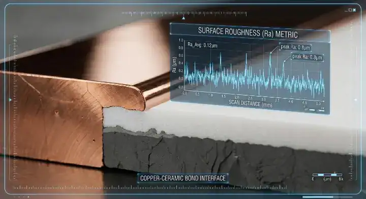
Spec #3: Surface Roughness (Ra) — Why It Matters for RF and Soldering?
Surface roughness (Ra) is a critical ceramic PCB specification that measures the microscopic smoothness of the board, where a DPC thin-film process achieves an ultra-smooth Ra < 0.5 μm, compared to a thick-film process which leaves a rougher Ra of 1–3 μm. For high-frequency RF applications, an increase of just 1 μm in Ra at 10 GHz can spike conductor transmission loss by 15% to 20% due to the skin effect.
How does roughness impact assembly? Beyond RF signal integrity, surface roughness dictates how well solder paste prints and flows. A rougher thick-film surface can cause erratic solder wicking, leading to inconsistent joint volumes on fine-pitch components.
- DPC (Thin Film): Ra < 0.5 μm (Required for RF and microwave).
- DBC (Direct Bond): Ra 0.5–1.0 μm (Standard for power modules).
- Thick Film: Ra 1–3 μm (Acceptable for basic circuits, poor for high-frequency).
Bottom line: If your design involves high-frequency RF signals above 5 GHz, you must strictly specify a DPC substrate with an Ra under 0.5 μm to prevent severe signal attenuation.
Spec #4: Dielectric Breakdown Voltage — Theoretical vs Tested Values?
When reading dielectric breakdown voltage on ceramic PCB specifications, factories quote a massive theoretical calculation (e.g., 15 kV/mm derived from material thickness), but the actual tested breakdown voltage is often much lower due to microscopic voids and surface defects. You cannot trust a theoretical calculation to protect a high-voltage circuit.
What is the real test? Instead of accepting a theoretical “15 kV/mm” line item, you must demand actual IPC-6012 compliance data. The factory must provide physical test reports showing the insulation resistance measures ≥ 100 MΩ when subjected to a 500V test charge.
- Theoretical Breakdown: A calculated marketing number based on perfect material thickness.
- Tested Insulation Resistance: The actual measured leakage current across the physical board.
- Red flag: The datasheet lists a massive kV number but provides no temperature or humidity testing conditions.
Bottom line: Ignore the theoretical kV/mm rating entirely and demand the factory’s physical IPC-6012 insulation resistance test data at 500V.
Spec #5: Thermal Cycling Endurance — How Many Cycles and at What Temperature Range?
A valid thermal cycling specification for a ceramic PCB must explicitly state the temperature range, the dwell time, and the exact number of cycles passed, rather than just printing a generic “Pass” on the datasheet. A rigorous automotive-grade test cycles from -40°C to +150°C, holding for 15 minutes at each extreme, and must prove the copper peel strength remains above IPC minimums after 1,000 cycles.
Why are vague claims dangerous? A supplier might claim their board “passes thermal cycling,” but they are referencing a weak industrial test of 500 cycles at a maximum of only 125°C. If you put that board into a 150°C environment, the copper will delaminate rapidly.
- Industrial Test: Typically 500 cycles from -40°C to +125°C.
- Automotive Test: Strictly 1,000+ cycles from -40°C to +150°C.
- Required Data: Must include copper peel strength data after the final cycle.
Bottom line: Reject any datasheet that simply says “Thermal Cycling: Pass”; demand the exact temperature limits, cycle count, and post-test peel strength metrics.
Spec #6: Dimensional Tolerances — Warpage and Outline Tolerances After Sintering?
Dimensional tolerance specifications for ceramic PCBs focus heavily on warpage after high-temperature sintering, where IPC-6012 Class 3 mandates that the board warpage must remain below 0.75% (measured as Length/750). Because ceramic is fired at extreme temperatures and bonded with heavy copper, achieving outline tolerances tighter than ±0.1–0.2 mm is difficult and drives up manufacturing costs significantly.
According to IPC (ipc.org) standards for high-reliability electronics, IPC-6012 Class 3 requires copper layer thickness tolerances of ±10% and strict warpage control. Why does warpage ruin assembly? If a ceramic substrate exceeds 0.75% warpage, the solder paste stencil will not sit flat during SMT assembly, causing massive solder bridging or insufficient paste on the pads. Reviewing our comprehensive ceramic PCB design rules DFM guide will help you set achievable tolerance expectations.
- Warpage limit: Must be strictly < 0.75% (L/750) per IPC-6012 Class 3.
- Outline profile tolerance: Standard is ±0.1 mm to ±0.2 mm.
- Thickness tolerance: Base ceramic thickness varies ±10%.
| Specification | Standard Tolerance | High-Precision (Premium Cost) | Assembly Impact if Failed |
|---|---|---|---|
| Warpage | < 0.75% | < 0.5% | Solder paste printing defects |
| Outline Dimension | ± 0.2 mm | ± 0.05 mm | Will not fit into CNC housing |
| Copper Thickness | ± 10% | ± 5% | Current carrying inconsistencies |
Choose standard tolerances if your board mounts with screws or clips. Choose high-precision outline tolerances only if you are press-fitting the ceramic into a tight machined housing.
Bottom line: Specify warpage limits strictly below 0.75% on your fabrication drawing; otherwise, your assembly house will struggle to print solder paste correctly.
Spec #7: Surface Finish Thickness — ENIG vs Silver Plating on Ceramic?
When reviewing surface finish ceramic PCB specifications, the standard reliable choice is ENIG (Electroless Nickel Immersion Gold) applied at 3–5 μm of nickel and 0.05–0.1 μm of gold, while Immersion Silver (0.1–0.5 μm) is used as a highly conductive alternative. You must explicitly define these thickness ranges on your drawing, as standard OSP (Organic Solderability Preservative) adheres very poorly to bare ceramic.
What goes wrong with surface finishes? ENIG provides excellent shelf life and flat pads for reflow soldering. Immersion silver offers better conductivity for wire bonding but oxidizes rapidly if exposed to standard factory humidity. Understanding ENIG surface finish quality ensures you avoid the dreaded “black pad” syndrome on expensive ceramic boards.
- ENIG: 3–5 μm Nickel + 0.05–0.1 μm Gold (Best for standard SMT reflow).
- Immersion Silver: 0.1–0.5 μm (Best for heavy wire bonding).
- Red flag: Avoid using OSP on ceramic substrates due to poor adhesion.
Bottom line: Specify ENIG with exact thickness parameters for standard SMT assembly, and strictly avoid OSP finishes on ceramic bases.
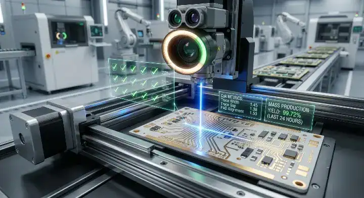
Spec #8: Minimum Line Width and Spacing — Process Limit vs Production Yield Limit?
The most dangerous ceramic PCB specification is the minimum line width; a factory stating a “50 μm minimum” is quoting their absolute process limit under lab conditions, whereas safe, high-yield mass production requires designing lines at 1.5 to 2 times that minimum. Designing right at the 50 μm limit often results in abysmal yield rates below 50% due to plating variations and edge roughness.
Engineers on EEVBlog regularly ask: “The factory said 50 μm minimum. I designed 55 μm traces, but my boards have open circuits. They blame my design, but I followed their rules. What happened?” We deal with this confusion constantly. We see this exact scenario cause yield problems at least once a month. The ’50 μm minimum’ in DPC means the photolithography can resolve it in ideal conditions—not that the heavy copper plating and ceramic flatness will cooperate in mass volume. Our rule of thumb: for DPC ceramic PCBs, design at 2× the stated minimum for 98%+ yield. If the factory says 50 μm, design at 100 μm for production. Use 75 μm only for prototype validation, and always demand the factory’s Cpk capability data. A Cpk ≥ 1.33 proves they can actually manufacture that width reliably.
- Prototype (5–10 pcs): You can test the absolute 50 μm limit.
- Mid-volume (100–500 pcs): Design at 1.5× the limit (75 μm) to stabilize yield.
- High-volume (1,000+ pcs): Design at 2.0× the limit (100 μm) for maximum cost-efficiency.
| Factory Stated Minimum | Safe Prototype Design | Safe Mass Production Design | Cpk Target |
|---|---|---|---|
| 50 μm / 50 μm | 50 μm | 100 μm | ≥ 1.33 |
| 75 μm / 75 μm | 75 μm | 150 μm | ≥ 1.33 |
| 100 μm / 100 μm | 100 μm | 200 μm | ≥ 1.33 |
Choose to design at the 2× safety margin if you are scaling straight to mass production. Avoid designing exactly at the factory’s stated minimum unless you are prepared to pay for high scrap rates.
Bottom line: Treat the stated minimum line width as a red flag process limit; multiply it by two for your actual production design rules to guarantee high assembly yields.
What Are the Most Frequently Asked Questions About Ceramic PCB Specs?
Why does my ceramic PCB thermal performance not match the datasheet? The most common reason is that datasheet thermal conductivity values are theoretical material maximums, not lot-specific measured values. Commercial AlN ceramic PCBs typically measure 150–180 W/m·K in production, not the theoretical 320 W/m·K. Always request ASTM E1461 laser flash test certificates for your specific production lot, and use those values in your thermal simulation.
What is a safe minimum trace width for DPC ceramic PCB production? Design at 2× the factory’s stated minimum line width for reliable production yield. If the factory lists 50 μm as their process minimum, use 100 μm as your production minimum. The stated minimum is achievable in ideal lab conditions but carries high defect risk in volume production. Always request Cpk data for the line width you’re designing — Cpk ≥ 1.33 indicates production-stable capability.
What surface finish should I specify for ceramic PCB assembly? ENIG (Electroless Nickel Immersion Gold) is the most reliable surface finish for ceramic PCBs going through reflow soldering. Specify nickel 3–5 μm and gold 0.05–0.1 μm per IPC-4556. Chemical silver is an option for cost-sensitive applications, but it oxidizes faster in storage and requires tighter humidity control. Avoid OSP on ceramic — the adhesion is poor on most ceramic surface finishes.
Trusting generic datasheet numbers without verification is the fastest way to fail a thermal simulation or ruin a production yield. We understand that translating theoretical material properties into physical mass-production reality is frustrating. At QueenEMS, we provide our clients with fully traceable, lot-specific test data and comprehensive DFM checks to ensure your design actually manufactures at scale. If you need clarity on your specifications, contact us to schedule a free engineering review of your ceramic Gerber files.
Written by the QueenEMS Engineering Team
Upload your files today · Free DFM check before production · Ship worldwide
Get your PCB prototypes in as fast as 24 hours. We handle FR4, Rogers, and Flex up to 60 layers — free prototypes for 2–4 layer boards, no minimum order.
Just upload your Gerber + BOM — we source every part, assemble, and inspect (AOI + X‑Ray) so you don't have to chase suppliers. Boards ship in as fast as 24 hours.