
Quick Answer: The standard PCB assembly order process takes 15 to 18 days for small batches, moving through 12 specific stages from DFM verification to final shipping. You can prevent 45% of unexpected factory delays by approving engineering queries within 24 hours and pre-checking your BOM for 16-week lead time components before submitting the files. Key takeaways:
- Component procurement runs parallel to bare board fabrication.
- Lead time officially begins only after you approve the final DFM report.
- Flying probe electrical testing is a mandatory validation stage.
- First Article Inspection catches 95% of placement errors early.
Table of Contents
- 1. What Is the PCB Assembly Order Process Timeline?
- 2. When Does the PCB Assembly Order Process Start?
- 3. Why Is DFM the First PCB Assembly Order Process Gate?
- 4. How Does Procurement Help the PCB Assembly Order Process?
- 5. What Approvals Drive the PCB Assembly Order Process?
- 6. How Does FAI Protect Your PCB Assembly Order Process?
- 7. Why Is Testing Mandatory in the PCB Assembly Order Process?
- 8. What Are the Top PCB Assembly Order Process Delays?
- 9. How Do Volume Sizes Change the PCB Assembly Order Process?
- 10. How Can You Track Your PCB Assembly Order Process?
You hit “submit” on your prototype files and suddenly hear absolutely nothing from the factory for a week. Wondering if your boards are stuck in customs or waiting on a single backordered resistor creates massive anxiety for hardware development teams. A highly transparent PCB assembly order process completely eliminates this blackout period by defining exact communication gates, required buyer approvals, and parallel manufacturing steps.
1. What Is the PCB Assembly Order Process Timeline?

The standard PCB assembly order process takes exactly 15 to 18 days to complete a 100-unit batch, advancing through 12 specific manufacturing and verification phases. You receive detailed documentation at five mandatory communication gates to verify production quality remotely.
The 12-Step Manufacturing Sequence
Most buyers assume fabrication and assembly happen sequentially, doubling the wait time. Here is the truth: professional factories run bare board fabrication and component sourcing concurrently to save weeks of waiting.
- Day 1-2: DFM Check and engineering queries.
- Day 3-10: Component procurement and bare board fabrication (parallel).
- Day 8-12: Surface mount assembly and reflow soldering.
- Day 12-14: AOI, X-Ray, and electrical testing validation.
Understanding Production Phases
You receive specific deliverables as your project clears each operational hurdle. Because the factory adheres to this strict sequence, which means no step begins until the previous one passes inspection, resulting in zero defects moving down the line.
| Timeline Stage | Factory Action | What the Buyer Receives |
|---|---|---|
| Day 1 – 2 | Design Verification | DFM report PDF |
| Day 3 – 10 | Fabrication & Sourcing | BOM shortage notification |
| Day 11 – 12 | First Article Build | FAI photos for approval |
| Day 15 – 18 | Final QC & Logistics | Test reports and tracking ID |
Reviewing the BOM shortage notification immediately keeps the production sequence moving without artificial pauses.
Key Takeaway: Bottom line: The 12-step timeline relies on parallel processing to finish small batch orders within 18 days.
2. When Does the PCB Assembly Order Process Start?
The PCB assembly order process officially starts its lead time clock on Day 0, which the industry defines strictly as the moment you resolve all engineering questions and approve the final BOM. The clock does not start on the day you submit your credit card payment.
Defining the Lead Time Trigger
Buyers frequently ask on the EEVBlog Forum: does the clock start when I pay, or when materials arrive? The direct answer is that lead time begins only after all technical ambiguities are eliminated from your CAD files.
Make no mistake:
- Unanswered DFM questions pause the clock immediately.
- A single missing part number prevents the procurement timer from starting.
- Waiting for your team to approve a capacitor substitution freezes the timeline.
How to Prevent False Starts
You must monitor your email inbox aggressively during the first 48 hours after payment. Factories cannot assume design intent, so they halt all operations until you explicitly authorize corrections to trace widths or pad sizes.
| Event Type | Does it Start the Clock? | Industry Standard Definition |
|---|---|---|
| Order Payment | No | Financial transaction only |
| File Upload | No | Awaiting engineering review |
| DFM Approval | Yes | “Day 0” for official manufacturing |
| Part Arrival | No | Internal factory milestone |
Providing a complete, scrubbed component list upfront prevents the clock from pausing on Day 2.
Key Takeaway: Bottom line: Your quoted 15-day turnaround begins exclusively after you sign off on the final engineering review.
3. Why Is DFM the First PCB Assembly Order Process Gate?
Design for Manufacturing (DFM) is the first gate in the PCB assembly order process because it catches 80% of footprint mismatches before a single piece of fiberglass is cut. Fixing a trace clearance issue during this software stage costs $0, while discovering it after fabrication demands a $2,000 board redesign.
Catching Footprint Errors Early
Engineers often export their Gerber files and immediately demand production without a factory review. Consider this reality: machine tolerances differ drastically from laboratory bench setups, requiring slight pad expansions to prevent tombstoning.
- DFM software checks minimum annular ring dimensions.
- Engineers verify that the drill sizes match your through-hole leads.
- Software flags copper pours that are too close to board edges.
The DFM Report Deliverable
You receive a formal document highlighting every design violation against the factory’s physical capabilities. Because the software identifies these spacing violations automatically, which means human oversight is eliminated, resulting in perfectly aligned solder masks.
| DFM Check Category | Target Specification | Risk if Ignored by Buyer |
|---|---|---|
| Trace Clearance | > 4 mil spacing | Electrical short circuits |
| Solder Mask | 2 mil expansion | Solder bridging on pins |
| Component Pads | Matches datasheet | Parts slide off during reflow |
Approving the solder mask expansion values guarantees that your fine-pitch microcontrollers will not bridge during wave soldering.
Key Takeaway: Bottom line: The DFM gate acts as a mandatory safety net that blocks unmanufacturable designs from wasting your raw materials.
4. How Does Procurement Help the PCB Assembly Order Process?
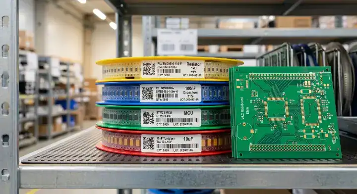
Parallel procurement accelerates the PCB assembly order process by ordering all electronic components on Day 1 while the bare boards are simultaneously chemically etched in another facility. This dual-track method cuts the total waiting time by at least 7 to 10 business days.
Solving Component Stock-Outs
Engineers frequently complain on Electronics Stack Exchange about components going out of stock immediately after order placement. To prevent this exact scenario, professional factories run a digital pre-check on your parts list immediately, notifying you of any 16-week lead times within 48 hours.
Pay close attention to this:
- Active parts are secured from Digi-Key or Mouser instantly.
- Passive reels are pulled directly from the factory’s internal inventory.
- Alternative parts are suggested for anything showing zero stock.
Approving Alternative Components
You must authorize any suggested part substitutions rapidly to keep the procurement track aligned with the fabrication track. Because the purchasing team secures the hard-to-find chips on Day 1, which means all materials arrive precisely on Day 10, resulting in zero idle time on the SMT line.
| Procurement Issue | Factory Action | Required Buyer Resolution |
|---|---|---|
| Out of Stock IC | Suggests drop-in replacement | Approve substitute within 24h |
| Obsolete Part | Flags BOM for redesign | Update schematic footprint |
| Long Lead Time | Sources from secondary broker | Approve broker pricing tier |
Authorizing cross-reference passive components from reputable Asian brands can bypass severe global supply chain shortages.
Key Takeaway: Bottom line: Parallel purchasing strategies guarantee that reels of components are waiting at the machine exactly when the bare boards arrive.
5. What Approvals Drive the PCB Assembly Order Process?
Specific buyer approvals dictate the PCB assembly order process pace, requiring your signature on DFM reports, part substitutions, and First Article photos to release the next manufacturing stage. Ignoring an email from your project manager directly causes your delivery date to slip backward by an equal number of days.
Why Buyer Response Time Matters
First-time buyers on Reddit r/PrintedCircuitBoard often stall their own projects because they do not realize the factory completely halts production while waiting for answers. Here is the truth: a modern manufacturing floor operates on tight schedules, and missing your slot means waiting for the next available machine opening.
- You must respond to engineering queries within 24 hours.
- You must approve or reject component swaps within 48 hours.
- You must verify golden sample high-resolution images same-day.
Managing the Communication Gates
You control the ultimate delivery speed by maintaining open communication channels with your account representative. Because the factory enforces these strict approval gates, which means no unverified changes occur, resulting in boards that match your exact design intent.
| Required Buyer Approval | Maximum Response Time | Consequence of Delay |
|---|---|---|
| DFM Query Response | 24 Hours | Lead time clock remains paused |
| BOM Substitution | 48 Hours | Components sell out to other buyers |
| FAI Photo Sign-off | 12 Hours | SMT line is reassigned to another job |
Treating factory emails as high-priority alerts directly protects your scheduled shipping deadline.
Key Takeaway: Bottom line: Your rapid responses to factory approval requests keep the production machines running on schedule.
6. How Does FAI Protect Your PCB Assembly Order Process?
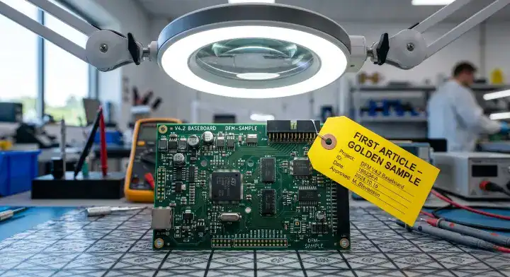
First Article Inspection (FAI) protects your PCB assembly order process by running 5 initial boards through the entire SMT line and verifying every component against your original CAD files. Approving this small sample batch prevents the factory from repeating a placement mistake 1,000 times over.
Validating the Golden Sample
A common customer mistake is skipping the FAI stage to save 48 hours, resulting in thousands of misaligned USB connectors. At QueenEMS, we mandate a 3D AOI and X-Ray inspection on every BGA joint during the First Article phase before we ever ramp up to full volume.
Make no mistake:
- FAI confirms the exact polarity of all diodes and LEDs.
- It verifies the thermal reflow profile perfectly melts the paste.
- It checks physical dimensions for exact enclosure fitment.
Locking the Quality Standard
You use the FAI report as the absolute quality benchmark for the remainder of the production run. Because we lock this standard after your photo approval, which means the machines operate on verified data, resulting in a 99.7% first-pass yield rate across our full production batches.
| FAI Verification Step | Defect Prevented | Impact on Mass Volume |
|---|---|---|
| Polarity Check | Backwards IC chips | Stops 100% board failure |
| Thermal Profiling | Cold solder joints | Eliminates manual rework |
| Component Values | Wrong resistor placed | Guarantees circuit function |
Signing the FAI release document legally authorizes the factory to consume the rest of your raw materials.
Key Takeaway: Bottom line: First Article Inspection acts as a physical safety barrier between prototype validation and mass production scale.
7. Why Is Testing Mandatory in the PCB Assembly Order Process?
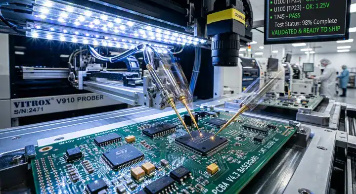
Electrical testing is a mandatory step in the PCB assembly order process because visual inspections alone cannot detect internal trace breaks or dead capacitors. Every single completed board must pass through a flying probe machine or custom testing jig to confirm strict electrical continuity before packaging.
Finding Invisible Failures
Automated Optical Inspection (AOI) only checks surface-level aesthetics, completely missing microscopic internal fractures in multi-layer boards. Consider this reality: skipping electrical validation ships visually perfect but functionally dead hardware directly to your end customers.
- Flying probe testers measure resistance across 1,000+ nodes in under 30 seconds.
- X-Ray machines calculate the exact voiding percentage beneath hidden BGA chips.
- Functional test jigs power on the board to flash specific firmware.
The Final Quality Gate
You receive a comprehensive test log file documenting the resistance and capacitance values of every net on the board. Because the robotic probes physically touch every copper pad, which means dead circuits are isolated instantly, resulting in zero defective units reaching the shipping dock.
| Testing Method | Defect Detected | Factory Stage |
|---|---|---|
| 3D X-Ray | BGA solder ball voiding | Immediately after reflow oven |
| Flying Probe | Open or short circuits | Final step before packaging |
| IC Programming | Blank microcontroller memory | Custom functional test stage |
Requesting the raw machine test logs provides undeniable proof that your batch meets IPC electrical standards.
Key Takeaway: Bottom line: Mandatory flying probe testing guarantees that your boards will actively conduct current exactly as engineered.
8. What Are the Top PCB Assembly Order Process Delays?
The most common delays in the PCB assembly order process are component stock-outs, incomplete Gerber files, and unexpected customs holds. Identifying these bottlenecks allows you to implement preventative actions before you submit your purchase order to the manufacturer.
Anticipating the Bottlenecks
Buyers often assume the factory controls the entire timeline, but the majority of delays originate from incomplete technical documentation provided at the start. Pay close attention to this: sending a BOM without specified manufacturer part numbers (MPNs) halts procurement immediately while the factory guesses your intent.
- Component stock-outs account for 45% of stalled projects globally.
- Missing pick-and-place centroid files force manual machine programming.
- Vague testing instructions lead to false failure reports on the floor.
Preventative Buyer Actions
You can eliminate these risks by running your BOM through a supplier API to verify active stock levels before sending it to the factory. Because the factory receives perfect documentation on Day 1, which means engineering holds are bypassed entirely, resulting in immediate fabrication scheduling.
| Primary Delay Cause | Delay Duration | Preventative Buyer Action |
|---|---|---|
| Stock-out Components | 2 to 16 weeks | List 3 approved alternatives per part |
| Missing Centroid Data | 2 to 4 days | Export XY coordinate files from CAD |
| Customs Inspection | 3 to 7 days | Provide accurate HS tariff codes |
Including specific HS codes on your commercial invoice prevents your finished package from sitting in a customs warehouse.
Key Takeaway: Bottom line: Providing complete data files and pre-checking part availability eliminates the most severe timeline bottlenecks.
9. How Do Volume Sizes Change the PCB Assembly Order Process?
Volume size dictates the PCB assembly order process speed, with prototypes completing in 5 to 10 days, while mass production batches stretch from 15 to 25 days. The timeline expands significantly for large orders because the factory transitions from flexible manual setups to rigid, high-efficiency automated fixtures.
Scaling Up the Timeline
Engineers transitioning from prototypes to their first mass run often expect the same 5-day quick-turn speed, which is physically impossible for 10,000 units. Here is the truth: high-volume runs require the creation of custom wave soldering pallets and complex ICT bed-of-nails fixtures.
- Prototype orders skip custom testing jigs to save upfront time.
- Small batches (100 units) balance automated SMT with standard probe testing.
- Volume orders (10,000 units) require 5 days just to manufacture custom tooling.
Time vs Volume Comparison
You must adjust your product launch schedule based on the specific batch size you authorize. Because high-volume orders utilize customized ICT fixtures, which means initial setup takes longer, resulting in testing speeds of 30 seconds per board instead of 5 minutes.
| Order Classification | Typical Volume | Realistic Production Timeline |
|---|---|---|
| Rapid Prototype | 5 – 25 Boards | 5 to 10 Business Days |
| Small Batch / NPI | 50 – 500 Boards | 10 to 18 Business Days |
| Mass Production | 1,000+ Boards | 15 to 25 Business Days |
Planning a 25-day buffer for mass volume orders prevents marketing teams from announcing unrealistic product shipping dates.
Key Takeaway: Bottom line: The order timeline stretches as batch volumes increase due to the creation of custom mass-manufacturing fixtures.
10. How Can You Track Your PCB Assembly Order Process?
You track your PCB assembly order process remotely through a dedicated project manager who sends mandatory stage-gate email updates and high-resolution production photos. Professional manufacturing partners replace the silent treatment with proactive, data-driven transparency at every critical milestone.
Demanding Production Visibility
You should never have to call a factory to ask if your boards are finished. Make no mistake: a transparent EMS provider supplies visual proof of life, sending you pictures of your bare boards the moment they exit the chemical etching baths.
- You receive tracking updates when bare boards pass their AOI scan.
- Account managers send alerts when the SMT line begins placing your parts.
- You review final pre-shipment photos of the boxes sealed with anti-static tape.
The Value of Dedicated Management
You rely on your account manager to act as your physical eyes and ears on the overseas factory floor. Because they provide real-time updates from the assembly line, which means you always know your exact order status, resulting in complete peace of mind.
| Tracking Mechanism | Visibility Provided | Buyer Benefit |
|---|---|---|
| Dedicated Manager | Single point of contact | Rapid issue resolution |
| Stage-Gate Emails | Real-time phase completion | Eliminates order anxiety |
| Pre-Shipment Photos | Visual proof of packaging | Validates shipping quantities |
Reviewing the pre-shipment photos guarantees that the factory used proper ESD-safe packaging before handing your boards to the courier.
Key Takeaway: Bottom line: Proactive stage-gate updates and dedicated account managers give you complete visibility into your offshore manufacturing timeline.
Frequently Asked Questions (FAQ)
Can I expedite my assembly order if I am facing a strict deadline? Yes, most factories offer expedited 24-hour to 72-hour quick-turn services for prototypes, provided your design is simple and all components are readily available in local stock. Expediting requires premium fees because the factory must disrupt their standard scheduling to prioritize your batch on the SMT line.
What’s the best way to handle components that have a 16-week lead time? You should authorize the factory to procure those specific long-lead components months in advance of your actual PCB fabrication order. Alternatively, you can redesign the specific circuit block to utilize a readily available cross-reference part from a reliable Asian semiconductor brand.
How do I know if the factory substituted my parts without permission? You demand high-resolution photos of the First Article Inspection (FAI) board before they run the remaining mass volume. By zooming in on the laser markings of the ICs on the physical board, you can cross-reference the parts against your original approved Bill of Materials to verify authenticity.
Does the timeline include shipping transit days? No, the standard 15-day manufacturing lead time strictly covers factory floor operations and stops the moment the box is handed to the logistics carrier. You must add 3 to 5 extra days for expedited international air freight, or up to 30 days for ocean freight transit.
Waiting in the dark for an offshore manufacturer to ship your hardware is a massive, unnecessary risk. A transparent sequence with clear communication gates guarantees you retain total control over your product launch schedule. At QueenEMS, we offer a Free DFM/DFA engineering review on every order, a 24-hour fastest turnaround capability, and full turnkey service from component sourcing to final testing.
Stop letting factory delays ruin your hardware deadlines. Partner with an EMS provider that values your timeline as much as your engineering. Contact us today to start your stress-free PCB assembly project.
Written by the QueenEMS Engineering Team
Upload your files today · Free DFM check before production · Ship worldwide
Get your PCB prototypes in as fast as 24 hours. We handle FR4, Rogers, and Flex up to 60 layers — free prototypes for 2–4 layer boards, no minimum order.
Just upload your Gerber + BOM — we source every part, assemble, and inspect (AOI + X‑Ray) so you don't have to chase suppliers. Boards ship in as fast as 24 hours.