
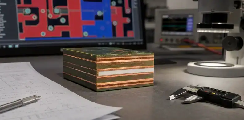
Buried capacitor PCB quotes slow down when the embedded capacitance is treated like a normal copper feature instead of a controlled stack-up function. The fabrication team has to understand the dielectric material, layer pair, active plane area, copper clearances, voltage condition, capacitance target, and test evidence before it can quote with confidence.
Quick answer: the seven mistakes that delay a buried capacitor PCB quote are vague dielectric notes, missing layer-pair information, uncontrolled active plane area, no voltage assumption, weak test requirements, informal CAM edits, and loose material substitution rules. If the RFQ package freezes those items before release, the supplier can separate manufacturing questions from design-intent questions much faster.
For buyers, this matters because embedded capacitance changes both the electrical model and the manufacturing risk. A small change in dielectric thickness or plane overlap can move capacitance enough to affect decoupling assumptions. A casual artwork edit can also change the effective capacitor area even when the board outline and layer count stay the same.
This checklist is written for procurement, hardware engineering, and DFM review teams that need a practical way to send buried capacitance work to a PCB supplier without triggering avoidable back-and-forth.
Table of Contents
- Mistake 1: Treating buried capacitance as a drawing note
- Mistake 2: Leaving the dielectric unnamed
- Mistake 3: Letting active plane area drift
- Mistake 4: Omitting voltage and reliability assumptions
- Mistake 5: Calling continuity test enough
- Mistake 6: Letting CAM edits change the capacitor
- Mistake 7: Accepting dielectric substitutions too casually
- FAQ
- How should buyers send the RFQ package to QueenEMS?
Mistake 1: Treating buried capacitance as a drawing note
A common RFQ problem is a stack-up note that says “embedded capacitance” or “buried capacitor layer” without defining what is controlled. That note tells the supplier the board is unusual, but it does not say which value must be protected during material selection, lamination review, CAM cleanup, or final inspection.
For a controlled build, the buried capacitor feature should be described as a design object. The RFQ should state the intended layer pair, dielectric thickness or material family, copper plane relationship, nominal capacitance target if one exists, and whether the value is a hard acceptance item or an engineering estimate.
The quote team also needs to know who owns decisions. If procurement sends the package but engineering owns the capacitance target, the RFQ should identify the approval contact before the supplier asks about material changes. That small detail often prevents a quote from waiting in the wrong inbox.
When the embedded layer is not defined as a controlled item, the safest supplier response is to hold the quote until the design intent is clarified. That delay is not administrative caution. It is a necessary check because a normal DFM cleanup step can become an electrical change.
The cleanest way to avoid this mistake is to add one short controlled-feature note beside the stack-up instead of scattering intent across fabrication notes, email comments, and schematic assumptions. The note should say that the named layer pair is an embedded capacitance feature, that dielectric and overlap changes require review, and that quote assumptions must call out any material or geometry deviation. This gives the supplier a single sentence to reference when CAM, purchasing, and engineering questions collide.
Mistake 2: Leaving the dielectric unnamed
The dielectric is the heart of a buried capacitance design. It controls separation between planes, affects capacitance density, and sets many of the process assumptions. If the RFQ only names a generic thin core or an old internal shorthand, the supplier must ask whether an exact material is required or whether an equivalent is acceptable.
The RFQ does not always need a single locked supplier material at the first conversation. It does need enough detail to quote the right class of material and to flag availability risk early. That means naming the approved material, an accepted equivalent list, or the dielectric constant and thickness range that engineering will accept.
| RFQ field | Why it matters | Quote-ready wording |
|---|---|---|
| Material name | Prevents the quote from using a generic thin dielectric | State the approved embedded capacitance material or approved equivalents |
| Dielectric thickness | Sets capacitance density and lamination assumptions | Provide nominal thickness plus accepted tolerance or range |
| Dielectric constant | Helps compare alternate materials | Include the value and measurement condition if engineering depends on it |
| Substitution rule | Avoids silent electrical changes | Say whether changes need written approval before quote release |
If the original material is obsolete or hard to source, say so in the RFQ. That allows the supplier to quote the design as an availability review instead of guessing whether a substitution is allowed.
For repeat builds, include the last accepted material and date code policy if the buyer has one. Some teams approve a material family but still require notification when the supplier changes thickness, resin system, or manufacturing location. Naming those boundaries in the RFQ helps the supplier decide whether the new quote is a repeat order, a controlled substitution, or a fresh engineering review.
Mistake 3: Letting active plane area drift
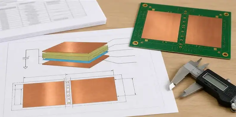
Buried capacitance depends on the overlap of active planes. The manufacturing file may show the planes, but the quote team still needs to understand whether those areas are fixed electrical features or ordinary copper pours that can be modified during CAM.
Plane splits, antipads, thermal relief rules, keepouts, and relief around tooling or test coupons can all affect useful area. A supplier may need to adjust copper for manufacturability, but the RFQ should define which changes are allowed without engineering review.
| Area question | Risk if unclear | Better RFQ instruction |
|---|---|---|
| Active plane outline | Capacitance estimate changes during CAM | Mark the plane area that must remain controlled |
| Splits and neck-downs | Local capacitance and current paths shift | Identify approved splits and no-change regions |
| Drill and via clearance | Antipads reduce overlap area | State whether CAM may resize clearances |
| Coupon placement | Test coupon may not represent the real plane pair | Define coupon relationship to the controlled stack-up |
The goal is not to freeze every square millimeter of copper if the product does not need that precision. The goal is to prevent accidental changes to the part of the copper system that engineering expects to behave like capacitance.
This is especially important when the board includes dense via fields, split power domains, or local keepouts near high-current components. Those features may be mechanically routine, but they can break the simple plane-overlap assumption used in early capacitance estimates. If the capacitance is used only as supporting decoupling, the allowed variation may be wide. If the design relies on a specific embedded value, the active area should be marked like any other controlled electrical geometry.
Mistake 4: Omitting voltage and reliability assumptions
Many RFQs state a capacitance target but do not state the voltage condition. That creates a gap because the supplier needs to review dielectric thickness, material selection, insulation margin, and test approach against the way the board will actually be used.
Voltage notes do not have to reveal confidential product details. A practical RFQ can provide the rail voltage, maximum expected differential voltage across the plane pair, any surge or qualification condition, and whether the embedded capacitance layer is tied to power integrity, EMI control, or another function.
If the design has a qualification plan, include the relevant acceptance language. If it is still an engineering build, say that clearly. A prototype quote can tolerate more open questions than a production quote, but the supplier must know which mode the buyer is requesting.
Three voltage details are worth naming in plain language:
- Rail voltage: give nominal and maximum voltage so the supplier knows whether the layer pair is a low-voltage decoupling feature or a higher-stress dielectric concern.
- Qualification condition: name the test standard or internal requirement when the dielectric needs extra reliability review.
- Acceptance basis: state whether capacitance is measured, calculated, or accepted by stack-up and material control.
When voltage and acceptance criteria are absent, the quote may look cheaper than the real build. That is the wrong kind of speed because the problem returns later as a DFM hold or production concession.
The RFQ should also separate normal operating voltage from screening or qualification voltage. A board may run at a modest rail voltage but still require a higher stress screen, or it may need only material and process confirmation for a low-voltage digital product. Stating the difference keeps the supplier from either under-reviewing the dielectric or over-quoting a test program that the buyer does not need.
Mistake 5: Calling continuity test enough
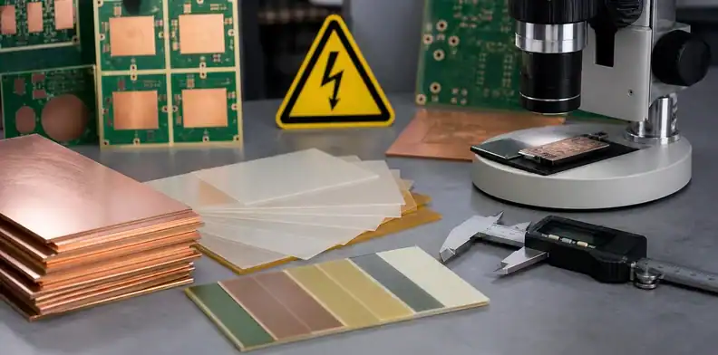
Open and short testing proves connectivity, but it does not prove the embedded capacitance value. If the buried capacitance is electrically important, the RFQ should say whether the buyer expects a calculated stack-up confirmation, a coupon measurement, a plane-pair measurement, or a certificate based on material and process controls.
The supplier may not be able to measure the exact in-circuit capacitance of every design in the same way. That is why the RFQ should define the evidence rather than assume the test method. A practical package can separate fabrication acceptance from engineering characterization.
| Evidence type | Best use | Limitation |
|---|---|---|
| Stack-up calculation | Early quote and DFM review | Depends on material data and active area assumptions |
| Coupon measurement | Production control | Coupon must represent the real plane pair |
| Plane-pair measurement | Engineering validation | Fixture and access method may be design-specific |
| Material certificate | Material traceability | Does not prove final board capacitance by itself |
If the value is still being tuned, mark the build as engineering validation. That gives the supplier room to quote fabrication feasibility while engineering decides what measurement should become the production baseline.
The acceptance language should be practical enough for production. For example, “confirm embedded capacitance by representative coupon and report result with shipment” is clearer than “verify capacitance” by itself. If the buyer only needs process traceability, say that. If engineering needs measured data from the first lot to tune a model, say that too. The quote can then include the right inspection labor, fixture assumptions, and reporting format.
Mistake 6: Letting CAM edits change the capacitor
CAM cleanup is normal in PCB fabrication, but buried capacitance makes some normal edits more sensitive. Copper balancing, plane smoothing, relief changes, drill clearance changes, and coupon edits can move the active area or change the dielectric relationship that the designer modeled.
The RFQ should identify which CAM edits need approval. This does not mean every tooling question has to return to the design team. It means the supplier should know which edits can be handled as manufacturability details and which edits touch the capacitor function.
| CAM change | Usually harmless when | Needs approval when |
|---|---|---|
| Copper smoothing | Outside controlled plane area | It changes the active overlap |
| Via antipad adjustment | Clearance remains in approved range | It removes meaningful active area |
| Coupon edit | Coupon remains representative | Coupon no longer matches layer pair |
| Plane split correction | It fixes an obvious file mismatch | It changes power or return plane intent |
For complex builds, add a named CAM approval step to the purchase process. That creates a controlled path for the supplier to ask targeted questions instead of sending a broad “please confirm stack-up” message late in the schedule.
A good CAM approval step does not have to slow the project. It can be a focused review of the embedded capacitance layer pair, the dielectric callout, the affected drill clearances, and any proposed coupon or copper adjustments. If the supplier can send a short hold list with marked screenshots, engineering can approve, reject, or revise the exact items that matter instead of rereading the full fabrication package.
Mistake 7: Accepting dielectric substitutions too casually
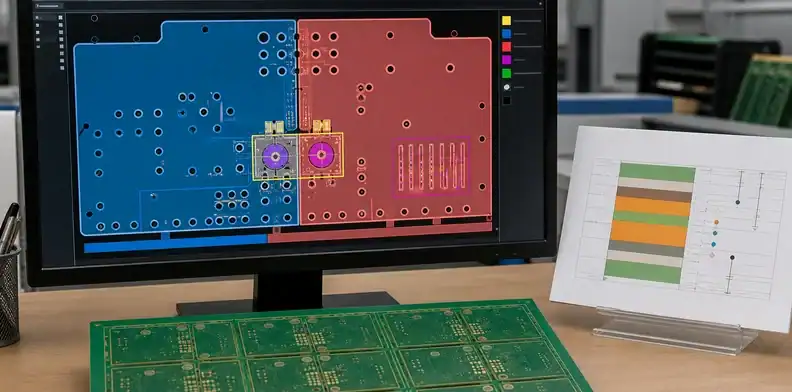
Material substitution is often where a buried capacitor PCB quote loses time. The buyer may want a fast alternate, the supplier may see a sourcing problem, and engineering may still need the original capacitance behavior. If the RFQ does not define the substitution rule, everyone has to pause.
A useful substitution rule states the original material, proposed alternate, accepted dielectric range, thickness range, layer pair, expected capacitance change, availability reason, and approval owner. It should also say whether the alternate applies only to prototype lots or becomes the production baseline.
Do not treat a buried capacitance dielectric like an ordinary laminate swap. Even when the mechanical build is possible, the electrical value may move. The quote should separate three decisions: whether the alternate can be fabricated, whether it meets the electrical target, and whether the buyer approves the change for this order.
For urgent builds, use a controlled exception. Ask the supplier to quote the original material and the proposed substitute as separate options, with the schedule and risk difference shown side by side. That keeps the commercial decision visible instead of burying it in an email thread.
The exception should expire unless the buyer deliberately promotes it. Prototype substitutions are useful when the team needs boards quickly, but they should not silently become production assumptions. Add a sentence such as “alternate dielectric approval applies to this prototype lot only unless engineering releases a revised stack-up.” That protects the next purchase order from inheriting a temporary decision.
FAQ
Is a buried capacitor PCB the same as a normal multilayer PCB with close planes?
Not always. Any close power and ground planes create some capacitance, but a buried capacitor PCB usually means the layer pair, dielectric, and active area are intentionally controlled for an electrical function. That controlled intent should appear in the RFQ.
Can the supplier choose an equivalent dielectric?
Only if the RFQ allows it. If the design depends on a specific capacitance density or qualification history, the buyer should require written approval before the supplier quotes or builds with an alternate dielectric.
Should every buried capacitance board include coupon measurement?
Not every board needs the same evidence. Engineering samples may use stack-up calculation plus a targeted measurement plan, while production builds may require a coupon, process certificate, or agreed acceptance report. The RFQ should state which evidence is required.
How should buyers send the RFQ package to QueenEMS?
QueenEMS should receive the stack-up page, dielectric datasheet or approved material name, active plane artwork, rail voltage note, capacitance or coupon requirement, quantity, and the exact substitution rule. Use the QueenEMS contact page and ask for a buried-capacitance quote-readiness review so the response can separate material availability, CAM holds, test evidence, and approval items before the PO is released.
If the files are not final, label them as an engineering RFQ and include the open decisions in the email body. That helps QueenEMS quote the current design honestly while returning a concise list of what must be frozen before production pricing, lead time, and acceptance evidence can be treated as stable.
Sources
- 3M, Embedded capacitance material technology
- IEEE Xplore, Embedded capacitance in printed circuit boards
Written by the QueenEMS Engineering Team
Upload your files today · Free DFM check before production · Ship worldwide
Get your PCB prototypes in as fast as 24 hours. We handle FR4, Rogers, and hybrid boards up to 40 layers in volume production, with advanced builds subject to engineering review — free prototypes for 2–4 layer FR-4 boards, no minimum order.
Just upload your Gerber + BOM — we source every part, assemble, and inspect (AOI + X‑Ray) so you don't have to chase suppliers. Boards ship in as fast as 24 hours.