
Are you struggling with unexpected short circuits during your SMT assembly phase? It is incredibly frustrating when a perfectly designed layout fails because of tiny solder bridges connecting adjacent pins. Just one small bridge can ruin an entire production run, leading to costly waste and missed deadlines. But here’s the kicker, most of these failures stem from a lack of understanding regarding proper solder resist application and quality standards. This guide provides a comprehensive solution by breaking down the technical nuances of the solder mask layer to ensure your boards are manufactured with the highest reliability. As a leading PCB assembly factory with over 100 machines, we have helped thousands of B2B clients optimize their designs for seamless factory-direct production.
1. What is solder mask and why do you need it?
A solder mask, also called solder resist or solder-stop coating, is a thin layer covering copper traces on a printed circuit board. What’s the real story? While most people recognize it as the vibrant green coating, its primary role is functional, acting as a barrier against environmental damage and assembly errors. At our facility, we emphasize that high-quality application is the first line of defense for industrial-grade electronic assembly.
- Preventing solder bridges between closely spaced pads.
- Shielding copper from corrosion and environmental contaminants.
- Providing electrical insulation between conductive traces.
- Reducing solder paste consumption during the reflow process.
| Function | Description | Impact on Quality |
| Bridge Prevention | Stops solder from flowing between pads | Reduces rework and failure rates +1 |
| Environmental Shield | Protects copper from moisture and air | Extends the lifespan of the PCB +1 |
| Insulation | Provides a dielectric barrier | Prevents electrical leakage |
Proper solder resist application is vital for B2B buyers who prioritize reliability and consistency over the lowest possible quote.
2. What is solder mask material and its composition?
The solder mask layer consists primarily of a specialized epoxy resin that offers excellent thermal and chemical resistance. This is where it gets interesting… The material must withstand the intense heat of reflow soldering without peeling or discoloring. Most professional pcb prototyping services utilize Liquid Photoimageable (LPI) inks because they provide the highest resolution for complex layouts.
Why are fillers and pigments added?
Pigments are added to give the board its characteristic color, while fillers control the viscosity and shrinkage of the ink. You might be wondering if the color affects performance; while green is standard, other colors like black or blue are often used for branding or specific light-blocking requirements.
| Material Component | Primary Purpose | Benefit to B2B Clients |
| Epoxy Resin | Adhesion and Protection | Long-term reliability |
| Photo-initiators | UV Curing | Precise pad alignment |
| Pigments | Color and Visibility | Easier inspection +1 |
Understanding the chemical composition helps engineers select masks that won’t outgas or degrade during high-temperature assembly cycles.
3. What is solder mask manufacturing process step-by-step?
The manufacturing process is a multi-stage operation requiring precision equipment and controlled environments. Here is the deal, a poorly applied mask can lead to “solder mask on pad” issues, which prevent components from bonding correctly. At our factory, we follow a strict sequence to ensure every board meets IPC standards.
How does the coating and exposure work?
The process begins with board cleaning to remove oils, followed by ink coating where the board passes through a vertical coater. Check this out, the thickness must be uniform across the entire surface to avoid uneven soldering heights.
What happens during developing and curing?
After exposure, the board enters a developing stage where unexposed ink is washed away, leaving the pads clear. Believe it or not, final thermal curing gives the mask its permanent durability. This level of process control is why our SMT assembly services maintain such a high yield rate.
| Process Step | Description | Critical Metric |
| Pre-Cleaning | Acid wash and brush cleaning | Surface cleanliness |
| UV Exposure | Pattern transfer via light | Alignment accuracy |
| Final Cure | 150°C oven baking | Adhesion strength |
Consistent execution in these steps prevents the common PCBA pain points of soldering instability and poor yield.
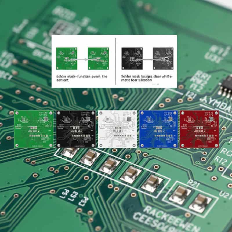
4. What is solder mask color and does it matter?
Choosing the right color is often more than a stylistic choice for B2B procurement managers. But wait, there’s more, different colors have varying levels of transparency and resolution. For instance, green ink allows for the easiest visual inspection, whereas black ink is used for consumer electronics where light leakage must be prevented.
Why is green the industry standard?
Green is favored because the human eye is most sensitive to green light, allowing inspectors to spot defects more easily.
- Superior contrast for manual and automated visual inspection (AOI).
- Higher resolution for fine-pitch components.
- Faster curing times in most production environments.
When should you choose black or white?
White masks are frequently used in LED applications to reflect light. Conversely, black masks are popular in robotics for a sleek look.
| Color | Best Use Case | Inspection Difficulty |
| Green | Standard Industrial/B2B | Low (Easy) |
| White | LED and Lighting | Medium |
| Black | Luxury/Light-sensitive | High |
The choice of color directly impacts the ease of quality control and the functionality of the final product.
5. What is solder mask type and which is best for you?
Not all coatings are equal, and the type you select depends on your board’s complexity. You might be wondering, “Should I use dry film or liquid?” For most B2B projects, Liquid Photoimageable (LPI) is the gold standard.
What is LPI (Liquid Photoimageable) solder mask?
LPI provides excellent contact with copper traces and allows for very small openings, perfect for high-density interconnects.
- High accuracy for fine-pitch pads.
- Available in matte or glossy finishes.
- Cost-effective for medium to high volumes.
When is dry film or epoxy used?
Dry film is applied using vacuum lamination. While less common, it offers uniform thickness across the board. But here’s the kicker, it is generally less effective at filling gaps between high traces than liquid versions.
| Mask Type | Application Method | Best For |
| LPI | Spray/Curtain Coat | High-density SMT |
| Dry Film | Lamination | Simple, large boards |
| Epoxy | Silk-screening | Low-cost prototypes |
Selecting the right type ensures that your board survives the high-precision BGA assembly process without failure.
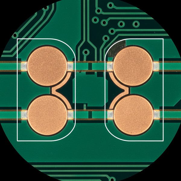
6. What is solder mask clearance in PCB design?
Clearance refers to the gap between the copper pad edge and the start of the mask. This is where it gets interesting… If this gap is too small, the mask might cover part of the pad, leading to poor solder joints.
How do you calculate proper clearance?
Most manufacturers require a clearance of at least 2-3 mils (0.05mm) to account for registration tolerances. You’ll want to hear this, if your design has “zero clearance,” you are essentially gambling on factory alignment precision.
- Always check factory DFM (Design for Manufacturing) guidelines.
- Standard clearance: 0.05mm to 0.1mm.
- Minimum mask dam: 0.1mm for reliable isolation.
What are the risks of insufficient clearance?
If the mask is too close, it can prevent solder paste from wetting the entire pad. What’s the real story? This results in “dry joints” that may fail after the product is shipped.
| Clearance Value | Result | Risk Level |
| < 2 mils | Solder mask on pad | High |
| 2 – 4 mils | Optimal alignment | Low |
| > 5 mils | Exposed copper traces | Medium |
Proper design clearance is the simplest way to avoid expensive rework and ensure soldering consistency.
Many standard factories struggle with sub-2 mil mask registration, forcing you to compromise on board density to avoid solder on pads. At QueenEMS, our industrial-grade LDI (Laser Direct Imaging) equipment easily handles extreme tight-pitch alignments. Not sure if your clearance is safe for mass production? Let our senior engineering team run a rigorous DFM review on your Gerber files—completely free.
7. What is solder mask dam and why is it vital?
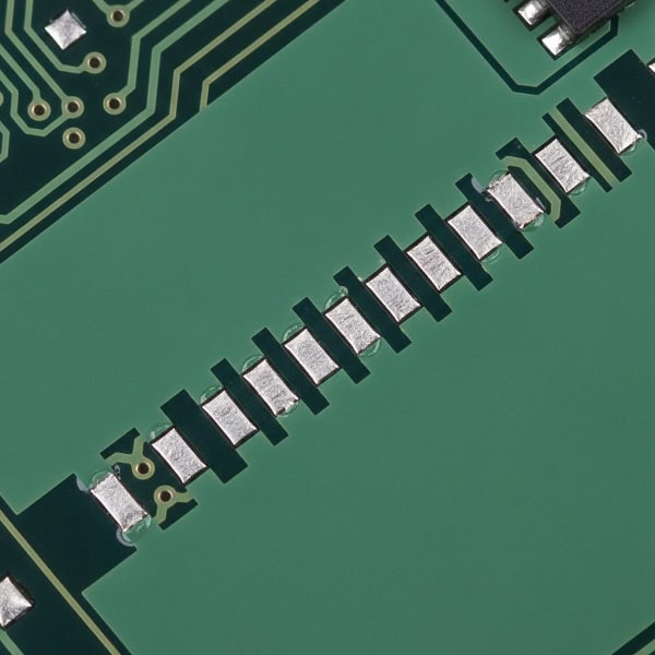
A solder mask dam is the narrow strip of mask between two adjacent copper pads. Ready for the good part? This dam is what actually stops solder from bridging. In high-density designs like robotics, stable dams indicate high factory capability.
What is the minimum dam width?
The minimum width depends on the ink color used. For green LPI, most factories can achieve a dam as small as 0.1mm.
- Green masks support the smallest dams.
- Black and white masks require larger dams.
- Crucial for fine-pitch IC packages.
What happens if the dam breaks?
If the dam is too thin, it may peel off during development. But wait, there’s more, without that barrier, molten solder will bridge the gap, creating a dead short.
| Feature | Minimum Size (Green) | Minimum Size (Black/White) |
| Mask Dam | 0.10 mm | 0.15 mm |
| Solder Opening | Pad size + 0.1mm | Pad size + 0.15mm |
Maintaining healthy dams is critical for high-yield manufacturing of complex industrial controllers.
A broken mask dam means a dead short, and inexperienced assemblers will often blame your layout. We don’t play that game. In production, our engineering matrix optimizes your solder dams upfront, and our 3D AOI catches 100% of bridging defects. Ready to stop worrying about SMT shorts and low yields?
8. What is solder mask inspection and quality standards?

Ensuring the mask layer meets quality standards is non-negotiable for high-reliability sectors like medical PCB assembly. Check this out, we use IPC guidelines to inspect for defects like peeling or misalignment.
What are common solder mask defects?
Visual inspection and AOI find issues such as “skip” or “bleeding”.
- Misregistration: Mask shifted, covering the pad.
- Blistering: Bubbles forming under the mask.
- Scratches: Damage exposing copper traces.
How do we test for adhesion?
The “Tape Test” is common, where tape is applied and pulled off quickly. You might be wondering, if any mask stays on the tape, the board fails the chemical bond test.
| Defect Type | Description | Industry Solution |
| Misregistration | Shifted mask layer | Laser Direct Imaging (LDI) |
| Blistering | Trapped air/moisture | Vacuum lamination |
| Peeling | Poor resin adhesion | Plasma cleaning |
Rigorous quality testing is the only way to ensure your PCBA isn’t a ticking time bomb of latent failures.
9. What is solder mask vs. silkscreen?
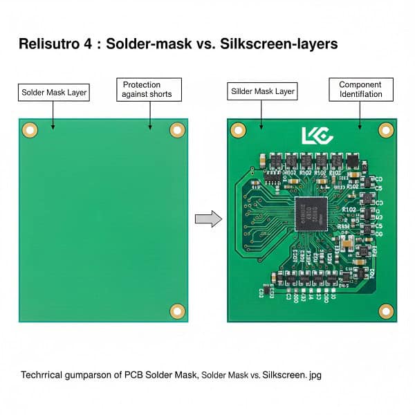
Many buyers confuse the solder mask layer with the silkscreen layer. Believe it or not, they serve completely different purposes. While the mask is a functional protective barrier, the silkscreen is informational.
What is the difference in material?
The mask is a rugged epoxy, while silkscreen ink is designed for high contrast and legibility.
- Solder mask: Protects copper, prevents bridges.
- Silkscreen: Labels components, provides instruction.
- Solder mask is applied first; silkscreen is printed on top.
Can silkscreen affect soldering?
Here’s the deal, if silkscreen is printed onto a solder pad, it prevents a good solder joint. This is why our engineering review team checks for “silk on pad” errors.
| Feature | Solder Mask | Silkscreen |
| Purpose | Functional Protection | Identification |
| Application | Coating/UV Exposure | Inkjet/Screen Printing |
| Location | Covers all traces | On top of the mask |
Understanding this distinction helps in creating cleaner, more professional board layouts.
10. What is solder mask design optimization for B2B?
Optimizing your design is the final step toward a successful product launch. You’ll want to hear this, engineering support during the design phase can reduce total cost by eliminating pitfalls.
How can you reduce manufacturing costs?
Using standard green LPI and following factory clearances results in the lowest price. This is where it gets interesting… specialized colors can add days to the schedule and increase price.
- Stick to standard colors (Green/White/Black).
- Use larger clearances to increase yield.
- Avoid “tenting” vias if used as test points.
Why use via plugging?
In some designs, filling vias with solder mask prevents solder from wicking to the other side, common in BGA assembly.
| Optimization Tip | Benefit | Production Impact |
| Use Standard Green | Lowest cost | Fastest Lead Time |
| Increase Clearances | Higher factory yield | Lower Unit Price +1 |
| Via Plugging | Prevents solder wicking | Higher Reliability |
Designing with manufacturability in mind is the fastest way to scale from a prototype to a full production run.
Theoretical design optimization is great, but execution is everything. Stop letting cheap quick-turn shops ruin your yield rates with sloppy mask application. Experience industrial-grade precision and speed with QueenEMS.
Conclusion
We have explored the vital role of the solder mask layer, from its chemical composition to the manufacturing steps and design best practices. By preventing solder bridges and protecting copper, the resist layer ensures your assemblies are reliable and durable. Whether you are managing pcb assembly for startups or scaling an industrial product, understanding these details is key to a successful partnership.
At Queenems, we transform your designs into high-performance hardware with engineering-driven execution and transparent communication. If you are ready to ensure your next production run is defect-free, contact us today to speak with our technical team. Our vision is to empower global innovators with a scalable and dependable supply chain advantage.
FAQ Section
Q1: Can I choose any color for my solder mask without affecting the price? No, while most factories offer green as the standard price, custom colors like purple often require a wash-up fee and can extend lead times. Green typically offers the best performance and cost-efficiency.
Q2: What’s the best way to handle vias in my solder mask design? It depends on your needs. Tenting (covering) vias protects them, while leaving them open allows for easier testing. For BGA designs, plugged vias are often best for preventing solder loss.
Q3: How do I know if my solder mask clearance is too small? If your manufacturer’s DFM report highlights “solder mask slivers” or “mask on pad” errors, your clearance is too small. A safe bet is to use a minimum clearance of 0.05mm.
Q4: How do I select between matte and glossy finishes? Glossy is more common and resistant to dirt, while matte is preferred by many engineers because it makes solder bridges easier to see during inspection.
Q5: What is the most important standard for solder mask quality? The IPC standard is the industry benchmark for PCB acceptability, providing specific criteria for solder mask adhesion, registration, and coverage quality.