
Are you struggling to squeeze more functionality into a shrinking device footprint while maintaining signal integrity? You might find that standard design rules are causing routing congestion and signal interference that halt your prototype’s progress. High-Density Interconnect (HDI) technology provides the solution by utilizing microvias and advanced lamination to increase component density without compromising performance.
In the modern electronics landscape, an HDI PCB is a circuit board with a much higher wiring density per unit area than conventional boards.
Why Should You Choose an HDI PCB for Your Next Project?
Choosing an HDI PCB is primarily driven by the need for smaller form factors and higher frequency signal demands in compact devices. When your design requires hundreds of pins in a tiny BGA package, standard through-hole technology simply runs out of space.
Is size the only factor?
Size reduction is significant, but the improved electrical performance is often the real winner for engineers. By using shorter interconnection paths, you reduce inductance and capacitance, which is critical for high-speed digital designs.
- Reduced board size and weight
- Enhanced signal integrity and electrical performance
- Accommodates high pin-count BGA components
But wait, there’s more.
How does it impact manufacturing?
While the design is complex, it often reduces the total layer count compared to a standard board trying to achieve the same density. Our PCB Design for Manufacturing (DFM) Review service ensures these complex layouts are actually producible at scale.
Key Takeaway: Moving to HDI allows for smaller, faster products while potentially simplifying the overall board structure if planned correctly.
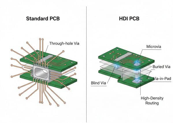
| Factor | Standard PCB | HDI PCB |
| Via Type | Through-hole | Microvias (Blind/Buried) |
| Trace/Space | > 4 mil | < 3 mil |
| Component Density | Low to Medium | Very High |
This comparison highlights why transitioning to high-density layouts is essential for cutting-edge electronics.
What Are the Core Components of HDI PCB Technology?
An HDI PCB relies on specific features like microvias, fine lines, and high-performance thin materials to function. These elements work together to create a 3D routing environment that goes far beyond traditional 2D surface routing.
What makes microvias so special?
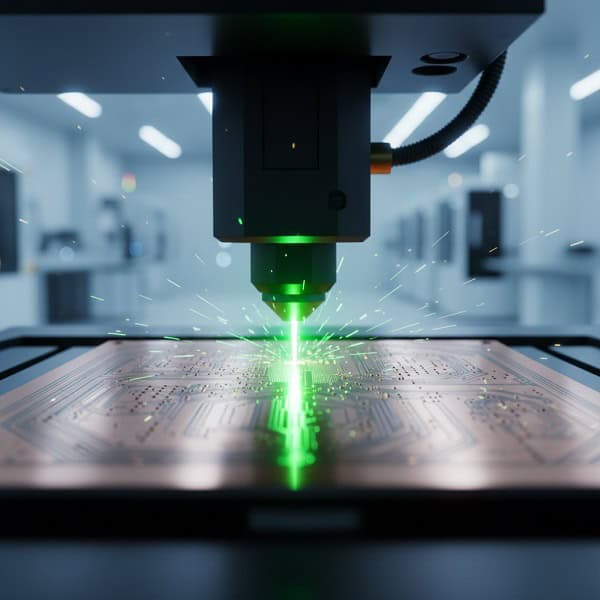
Microvias are the heart of this technology, typically having a diameter of less than 150 microns. Because they take up so little space, you can place them directly in component pads, freeing up massive amounts of routing real estate.
- Laser-drilled for extreme precision
- Low aspect ratios for better plating reliability
- Supports via-in-pad structures
Think about the possibilities.
How are layers interconnected?
Unlike standard boards, these utilize sequential buildup where layers are added and drilled in stages. This allows for complex Microvia PCB architectures like “stacked” or “staggered” vias across multiple layers.
Key Takeaway: Understanding the physical building blocks of HDI helps you design boards that maximize space without sacrificing structural integrity.
| Feature | Standard Via | Microvia |
| Drill Method | Mechanical | Laser |
| Typical Diameter | 0.2mm – 0.5mm | 0.05mm – 0.15mm |
| Pad Size | Large | Extremely Small |
The move to laser-drilled features is what truly defines the leap in manufacturing capability.
How Do Microvias Enhance Your HDI PCB Design?
Integrating microvias into an HDI PCB design allows for significant improvements in routing density and signal paths. By replacing bulky through-holes with tiny, precise laser-drilled holes, you eliminate the “stubs” that often cause signal reflections.
What are the different microvia types?
You generally work with three types: blind vias, buried vias, and microvias. Blind vias connect an outer layer to an inner layer, while buried vias connect two inner layers without ever reaching the surface.
- Blind vias: Visible on only one side
- Buried vias: Hidden entirely within the core
- Via-in-pad: Placed directly under component leads
It gets even better.
Why use via-in-pad?
This technique allows you to place a via directly in the SMT pad, which is essential for high-pitch BGA Assembly Services. It minimizes the space required for “dog-bone” fanouts, allowing you to pack components much closer together.
Key Takeaway: Mastering microvia placement is the most effective way to solve routing bottlenecks in high-speed, compact designs.
| Via Strategy | Routing Space | Signal Quality | Cost Impact |
| Through-hole | Minimal | Average | Low |
| Staggered Microvias | High | Excellent | Moderate |
| Stacked Microvias | Maximum | Excellent | Higher |
Utilizing the right via strategy is a balance between performance requirements and production budget.
What Is the Sequential Buildup Process in HDI PCB?
The manufacturing of an HDI PCB follows a sequential buildup (SBU) method rather than a single-press lamination. This means the factory creates a core, then adds layers one or two at a time, drilling and plating them before adding the next.
How many cycles are typical?
Most designs use a “1+N+1” or “2+N+2” structure, where “N” is the core and the numbers represent the buildup layers. Each “plus” represents an extra lamination and laser drilling cycle, which adds to the complexity and time.
- Stage 1: Core fabrication and through-hole drilling
- Stage 2: First buildup layer lamination and laser drilling
- Stage 3: Successive layers and final plating
The process is fascinating.
Does this affect lead times?
Yes, because each cycle requires a trip through the lamination press and the laser driller, it takes longer than a standard Multi-Layer PCB Assembly. However, the result is a level of density that is impossible to achieve any other way.
Key Takeaway: Understanding the buildup cycles helps you estimate manufacturing costs and avoid unnecessary complexity that doesn’t add value.
| Build Style | Cycles | Complexity | Use Case |
| 1+N+1 | 1 | Standard HDI | Smartphones |
| 2+N+2 | 2 | High Complexity | Tablets/Medical |
| Any Layer | Multiple | Maximum | High-end Computing |
Choosing the simplest buildup that meets your density needs is the best way to manage costs.
What Are the Critical DFM Rules for HDI PCB Designs?
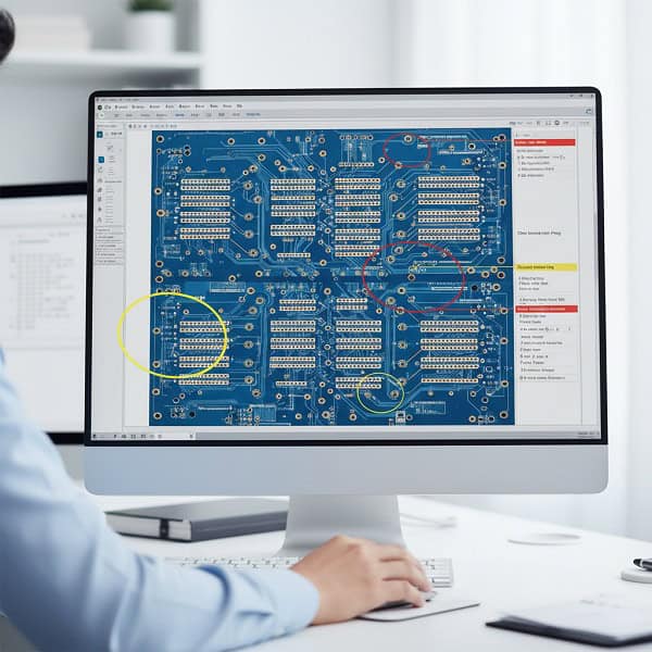
Applying strict DFM rules to your HDI PCB is the difference between a prototype and a mass-producible product. Because the tolerances are so tight, even a tiny misalignment in the laser or a slight over-etch can ruin an entire panel.
What is the most common error?
Annular ring breakouts are the most frequent issue, occurring when the pad around a via is too small. You must ensure your landing pads are large enough to account for the registration tolerances of the laser and lamination press.
- Minimum annular ring requirements
- Aspect ratio limits (depth vs. diameter)
- Trace-to-pad clearances
You need to be careful.
How do we help?
We offer a comprehensive PCB Design for Manufacturing (DFM) Review specifically for high-density projects. This prevents common pitfalls like “acid traps” or insufficient copper plating in microvias before you spend money on production.
Key Takeaway: Designing with manufacturing tolerances in mind from day one is the fastest way to get your product to market.
| DFM Check | HDI Standard | Risk if Ignored |
| Aspect Ratio | < 1:1 for Microvias | Poor plating/Failure |
| Annular Ring | Min 2 mil | Breakout/Open circuit |
| Trace/Space | 2-3 mil | Shorts/Crosstalk |
Following these guidelines ensures that your complex design is as robust as it is innovative.
Conclusion
Mastering the complexities of high-density design is no longer optional for engineers working on the next generation of electronics. This guide has explored how microvias, sequential buildup, and meticulous stackup planning transform a standard board into a high-performance HDI PCB. By focusing on DFM and choosing the right materials, you can overcome routing bottlenecks and deliver a reliable product.
We’ve solved these challenges for hundreds of clients, and we’re ready to help you too. Whether you’re looking for expert HDI PCB fabrication or a comprehensive design review, our team is here to ensure your project’s success. Contact us today to discuss your specific requirements and get a professional engineering quote within 2 hours.
Our vision is to bridge the gap between complex engineering and reliable manufacturing, making advanced PCB technology accessible to innovators worldwide.
FAQ
Can I use standard FR4 for all HDI designs?
Generally, no. While some simple HDI boards use standard FR4, most high-density designs require high-Tg or low-loss materials to handle the thermal stress of multiple lamination cycles and ensure signal integrity.
What’s the best way to reduce cost on an HDI board?
Minimize the number of buildup cycles. A “1+N+1” design is significantly cheaper than a “2+N+2” or “3+N+3” because it requires fewer laser drilling and lamination steps.
How do I know if my design actually needs HDI?
If you are using BGA components with a pitch of 0.5mm or smaller, or if you cannot route your board without exceeding 8-10 layers of standard technology, you likely need to transition to HDI.
How do I prepare for my first HDI project?
Talk to your manufacturer first. Getting their specific design rules for laser drilling and layer registration will save you hours of layout rework.
What is the minimum via size for most HDI factories?
Most professional factories can reliably drill microvias down to 0.1mm (4 mil), with advanced facilities capable of 0.075mm (3 mil) or smaller depending on the material thickness.