
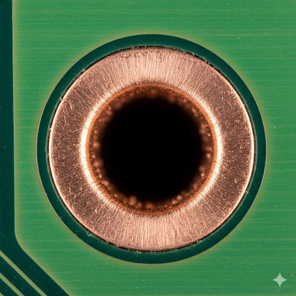
An annular ring represents that critical copper area which remains around a drilled hole after your circuit board manufacturing process finishes successfully. Sourcing high-quality printed circuit boards often feels simple until you encounter unexpected connectivity failures or signal interruptions during final testing phases. These hidden defects usually stem from tiny drill misalignments which completely sever copper connections between different layers within your expensive hardware prototypes. One small shift during the drilling phase turns a functional board into scrap metal while wasting thousands of dollars and weeks of development time. We provide expert engineering support and precision manufacturing at Queenems to ensure your annular ring pcb meets strict IPC standards for maximum reliability. Our factory utilizes advanced 100+ machine configurations to maintain tight tolerances and prevent common defects like breakout or tangency in every production batch.
1. What is an annular ring pcb?

An annular ring pcb refers to that finished width of copper pad encircling any plated through-hole or via structure on your board. This specific feature serves as the vital conductive bridge between your electrical traces and vertical paths connecting multiple layers together during operation. But here’s the kicker… without a properly sized ring, your signals might never reach their destination due to physical gaps created during aggressive etching. Professionals must account for manufacturing tolerances early because even advanced drills possess slight mechanical variations when piercing dense fiberglass substrates during high-speed production.
How does copper surround your via?
Every conductive hole through your board necessitates a surrounding copper land ensuring electrical continuity remains robust throughout your entire product lifecycle. Your design files should specify enough copper area so that finished plating adheres securely inside the barrel without peeling away during soldering. What’s the real story? Thin rings often lead to weak mechanical joints which fail under thermal stress when your device operates in demanding industrial environments. These failures cause intermittent signals that are extremely difficult to diagnose without expensive laboratory equipment or destructive testing methods.
● Circular copper pads provide the best surface area for drill alignment. ● Minimum widths vary based on your chosen IPC class requirements. ● Thicker rings improve overall heat dissipation for high-power circuits.
Key Takeaway: Proper ring definition guarantees your electrical signals transition between layers without encountering high resistance or total circuit failure during use.
Summary Table: Definition Basics
| Component | Function | B2B Impact |
|---|---|---|
| Pad Diameter | Outer boundary | Sets limits for drill |
| Drill Size | Internal hole | Determines finished path |
| Ring Width | Conductive bridge | Ensures signal reliability |
2. Why is the annular ring width critical?
The width of your annular ring pcb directly determines how much tolerance your manufacturer has before a drill bit wanders outside the copper boundary. Large widths provide a safety net that absorbs mechanical errors while maintaining a full circle of metal around every single plated through-hole. Ready for the good part? Using wider rings significantly boosts your manufacturing yield because fewer boards get rejected during final visual and electrical inspection stages. If you choose extremely small widths, even a microscopic drill deviation might result in a complete disconnect between surface traces and internal power planes.
Can small rings handle high current?
High-current applications require substantial copper mass to prevent localized overheating which can delaminate your fiberglass substrate or melt conductive traces during operation. Narrow rings possess higher electrical resistance that generates heat when large amounts of energy flow through the vertical paths of your multilayer designs. This is where it gets interesting… designers often overlook this thermal aspect while focusing solely on space savings for compact consumer electronics or high-density projects. Ensuring adequate copper volume around vias allows for better heat spreading and prevents the formation of hot spots that degrade component lifespan.
● Wider copper areas reduce the risk of pad lifting during rework. ● Thick rings facilitate better solder fillets during the assembly process. ● Signal integrity improves when the transition area remains consistent and solid.
Key Takeaway: Optimizing width prevents thermal failures and mechanical fatigue by providing a stable foundation for every electrical connection on your board.
Summary Table: Width Importance
| Metric | Small Width | Large Width |
|---|---|---|
| Manufacturing Risk | Very High | Very Low |
| Current Capacity | Limited | High |
| Rework Durability | Poor | Excellent |
3. How do you perform an annular ring calculation?
Performing an annular ring pcb calculation involves subtracting the drill diameter from your outer pad diameter and then dividing that final result by two. This mathematical formula represents the actual width of copper remaining on one side of the hole after the drilling process finishes successfully. You might be wondering… why we divide by two instead of just using the total difference between circular dimensions provided in your Gerber files. This step is necessary because the drill removes metal from the center, leaving equal amounts of copper on every side of the resulting hole.
Does drill wander change your math?
Mechanical drills never strike the exact center of a pad perfectly every time due to material shrinkage and machine movement during the fabrication process. Your calculations must include a “fabrication allowance” that compensates for these real-world deviations without compromising minimum ring requirements specified by IPC standards. Here’s the deal… if your math ignores these manufacturing variances, you might end up with boards that look perfect in CAD but fail in reality. Professional engineers always calculate based on finished hole sizes rather than the initial drill bit diameter to ensure accuracy throughout the build.
● Always use the finished hole size for your final calculations. ● Factor in plating thickness which adds metal back to the walls. ● Check your CAD settings to ensure pad diameters match your specs.
Key Takeaway: Accurate math ensures your design remains manufacturable across different factories without requiring constant modifications or expensive custom tooling during production.
Summary Table: Calculation Formula
| Parameter | Variable | Calculation Step |
|---|---|---|
| Pad Diameter | (L) | Measured outer edge |
| Hole Diameter | (H) | Finished drill size |
| Ring Result | (R) | (L – H) / 2 |
4. What causes annular ring breakout?
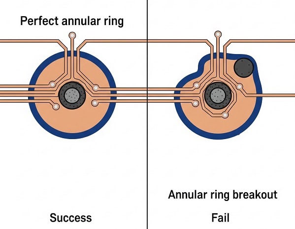
Annular ring breakout occurs when the drill bit strikes your board so far from center that it penetrates outside the copper pad boundary. This defect creates a crescent-shaped gap where the trace meets the hole, often leading to total loss of electrical connectivity between layers. Wait, there’s more… even if the connection remains partially intact, the reduced contact area creates a high-resistance bottleneck that can burn out under load. Material expansion during the lamination process often shifts inner layers slightly, making perfect alignment nearly impossible for high-layer count circuit board builds.
How does drill registration affect breakout?
Registration refers to how accurately various layers of your board align with each other before heavy drilling machines start their high-speed work. If the lamination process causes even minor shifts, the drill might hit the top pad perfectly while completely missing targets on internal planes. Don’t miss this… professional manufacturers like us use X-ray alignment systems to compensate for these internal shifts before we begin any drilling operations. These advanced systems allow us to map the actual location of internal pads and adjust the drill path for every individual board panel.
● 90-degree breakouts are often acceptable for Class 1 consumer products. ● Class 3 medical boards require zero breakout for maximum safety. ● Breakout typically happens at the trace-to-pad junction most frequently.
Key Takeaway: Understanding breakout causes allows you to design larger pads that accommodate unavoidable manufacturing shifts without sacrificing final product quality or reliability.
Summary Table: Breakout Types
| Defect Level | Description | Usage |
|---|---|---|
| Tangency | Drill touches edge | Acceptable Class 2 |
| Breakout | Hole exits copper | Reject Class 3 |
| Preferred | Centered hole | Best Reliability |
5. How do teardrop pad PCB designs prevent failures?

A teardrop pad PCB design adds extra copper at the junction where a thin trace meets a circular pad to prevent breakage. This triangular reinforcement strengthens the connection point and ensures even a significant drill shift won’t completely disconnect the signal path from its via. But wait, it gets better… teardrops also reduce amount of stress concentrated at these sharp corners during thermal cycles experienced during the wave soldering process. By smoothing the transition from trace to pad, you create a more robust structure that handles mechanical vibrations much better than standard configurations.
Can teardrops save your board?
If your layout requires tight spacing where large pads simply won’t fit, adding teardrops serves as an effective insurance policy against manufacturing defects. They provide extra copper area exactly where the drill is most likely to cause a breakout, effectively increasing your manufacturing window safely. Think about this… most modern CAD tools can automatically generate these shapes across your entire board with just a few clicks in the settings. This simple design adjustment can save you thousands in rework costs by drastically reducing the number of boards that fail electrical testing.
● Teardrops prevent “acid traps” from forming during the etching stage. ● Signal transitions become smoother which helps with high-speed data. ● Mechanical strength increases significantly at every via connection point.
Key Takeaway: Implementing teardrops is a low-cost design improvement that drastically increases the survivability of your circuits during both fabrication and field use.
Summary Table: Teardrop Benefits
| Feature | Without Teardrop | With Teardrop |
|---|---|---|
| Drill Tolerance | Very Tight | More Flexible |
| Connection Strength | Moderate | Very Strong |
| Manufacturing Yield | Standard | Optimized |
6. Can I avoid tangency in manufacturing?
Tangency occurs when the edge of the drilled hole perfectly aligns with your outer edge of the copper pad without actually breaking out. While IPC Class 2 standards generally allow for tangency, it represents the absolute limit of acceptable manufacturing and leaves no room for further errors. Check this out… you can avoid this risky condition by increasing your pad diameters by just a few mils to provide a comfortable buffer. Professional designers always aim for a “preferred” condition where a full ring of copper remains visible around the entire circumference of every finished hole.
Does plating thickness matter?
The thickness of copper plated inside the hole actually reduces the final diameter of opening, which can sometimes hide a near-tangency condition during inspection. However, the initial drill size is what matters most because that determines the physical area of copper removed from your carefully designed pads. You might be wondering… if choosing a smaller drill size is always the best solution for avoiding tangency in high-density board layouts globally. Smaller drills are more fragile and expensive to use, so balancing drill size with pad diameter is a critical skill for any hardware engineer.
● Tangency is often a sign your design is too tight for the factory. ● Increasing pad size by 2-4 mils usually eliminates most tangency issues. ● Consistent tangency across a batch suggests a systemic machine calibration error.
Key Takeaway: Aiming for more than the minimum ring width keeps your project safely away from tangency limits and ensures a higher pass rate.
Summary Table: Tangency vs. Breakout
| Condition | Definition | Status |
|---|---|---|
| Tangency | Edge to Edge | Marginal |
| Breakout | Outside Edge | Failed |
| Sufficient Ring | 360 Degree Cover | Success |
7. What is the best strategy for PCB via design?
Designing vias correctly requires a careful balance between electrical performance, thermal management, and practical limitations of modern circuit board fabrication equipment today. You must choose a pad size that is large enough to support the drilling process while remaining small enough to allow efficient routing. What’s the real story? Over-sized vias can block routing channels on inner layers, while under-sized vias significantly increase the risk of manufacturing defects and signal loss. Using a standardized set of via sizes across your entire design helps the factory optimize their drilling sequence and reduces your time.
Should you use filled vias?
Filled vias offer better thermal conductivity and allow you to place components directly on top of the hole, which is known as via-in-pad. This advanced method saves significant board space but requires extra manufacturing steps like epoxy filling and copper capping to create a flat surface. Here’s the deal… if your design doesn’t strictly require these features, sticking to standard open vias will save you a considerable amount of money. Every extra process step added to your fabrication quote increases the lead time and the potential for manufacturing errors during production.
● Tent your vias with solder mask to prevent shorts and solder wicking. ● Use thermal vias under power components to move heat to internal planes. ● Keep via-to-via spacing consistent to avoid drilling through thin walls.
Key Takeaway: Consistent and well-planned via designs simplify the fabrication process and lead to more predictable electrical performance in your final hardware products.
Summary Table: Via Design Choices
| Via Type | Advantage | Cost Impact |
|---|---|---|
| Standard | Simple to make | Lowest |
| Via-in-Pad | Saves Space | High |
| Microvia | High Density | Very High |
8. How does drill registration affect your yield?
Drill registration refers to the precision with which a machine can place a hole at exact coordinates specified in your digital files. Even the best industrial drills have a tolerance range, usually within a few microns, which can lead to slight misalignments when processing thousands. Ready for the good part? Understanding this limitation allows you to design your copper pads with enough “slack” to absorb these small placement errors. If your pads are too small, even a tiny registration error will result in the drill bit missing the target copper area entirely.
Does board size impact accuracy?
Large circuit boards are more susceptible to material expansion and contraction during the intense heat of the lamination process, which can shift targets. This “scaling” effect means that holes near the edges of a large panel might be less accurately placed than those located closer. This is where it gets interesting… we use sophisticated software to analyze these distortions and adjust the drill paths in real-time to compensate. This ensures that every hole hits its intended copper pad even on large, high-layer count boards that have undergone significant thermal stress.
● Multi-layer boards require more complex registration than simple boards. ● Fiducial markers help machines align precisely with your copper layers. ● Material choice impacts how much board dimensions change during heat.
Key Takeaway: Designing with registration tolerances in mind ensures your boards remain functional even when the manufacturing process pushes the limits of accuracy.
Summary Table: Registration Factors
| Factor | Impact on Precision | Solution |
|---|---|---|
| Machine Calibration | High | Regular Service |
| Material Stability | Medium | High-Tg FR4 |
| Board Size | High | Compensation |
9. Does aspect ratio impact annular rings?
Aspect ratio represents the relationship between the thickness of your circuit board and the diameter of its smallest drilled hole during fabrication. Higher aspect ratios make the plating process much more difficult because the chemical fluids struggle to flow through long, narrow holes effectively. Wait, there’s more… if the plating inside the hole is uneven or too thin, the mechanical bond with the annular ring becomes weak. This can lead to barrel cracking during the assembly phase when the board is exposed to high temperatures for extended periods of time.
Can you optimize plating quality?
Ensuring that your through-hole plating is robust requires a stable ring that acts as an anchor for the copper barrel inside the hole. If the ring is too small, the plating may peel away during thermal expansion, causing intermittent electrical connections that are difficult to fix. Don’t miss this… keeping your aspect ratio below 10:1 for standard production ensures that the plating chemistry can deposit a consistent layer of copper. This leads to a much stronger connection between the hole wall and the surface pads, significantly improving the overall reliability of your device.
● Aspect ratios above 12:1 require specialized equipment and chemical processes. ● Thicker copper plating increases the current-carrying capacity of your vias. ● Reliable plating is essential for boards used in high-vibration environments.
Key Takeaway: Balancing your aspect ratio with adequate ring size ensures that every hole on your board is plated correctly and remains durable.
Summary Table: Aspect Ratio Effects
| Ratio | Plating Ease | Reliability |
|---|---|---|
| < 8:1 | Very Easy | Highest |
| 10:1 | Standard | Good |
| > 12:1 | Difficult | Risky |
10. What are IPC Class 2 requirements for rings?
IPC Class 2 standards represent the industry baseline for most commercial and industrial electronic products, requiring a minimum finished annular ring width. These rules allow for some minor drill deviation, including tangency, as long as the electrical connection remains secure and minimum metal width exists. But here’s the kicker… if your product is intended for critical applications like aerospace or medical life-support systems, you must follow Class 3. Class 2 is the most common choice for B2B projects because it balances manufacturing cost with a very high level of performance.
How do you verify compliance?
Verification usually involves cross-sectioning a sample board from the production batch and examining holes under a microscope to measure actual copper remaining. We provide detailed inspection reports and certificates of compliance to ensure every board we ship meets specific standards requested by our customers. What’s the real story? Many low-cost factories skip these verification steps, which can lead to hidden defects that only appear after months in the field. Working with a certified partner ensures that your hardware is built to professional standards that protect your brand reputation.
● Class 2 allows for a 90-degree breakout in some specific circumstances. ● External rings must usually be at least 2 mils (0.05mm) for Class 2. ● Internal rings often have slightly different requirements than external ones.
Key Takeaway: Adhering to IPC Class 2 guidelines provides a globally recognized benchmark for quality that ensures your hardware meets professional expectations.
Summary Table: IPC Class Comparison
| Requirement | IPC Class 1 | IPC Class 2 | IPC Class 3 |
|---|---|---|---|
| Quality Level | General | Dedicated | High Reliability |
| Min Ring Width | Lowest | Moderate | Highest |
| Breakout Allowed | Yes | Marginal | No |
Conclusion
Mastering the complexities of annular ring design is essential for producing reliable hardware that meets modern B2B quality standards effectively. By implementing accurate calculations, using teardrop pads, and adhering to strict IPC guidelines, you can significantly reduce manufacturing risks and improve long-term performance. We covered everything from basic definitions to advanced aspect ratio considerations to help you optimize your next high-performance circuit board project. Our team at Queenems is dedicated to providing precision engineering and factory-direct solutions that bring your complex designs to life without costly defects. If you need expert support for your next PCB project, please contact us today for a professional consultation and fast quotation. We stand behind every board we manufacture, ensuring that your business stays ahead with reliable and scalable electronic solutions that drive success.
FAQ
Q1: Can I use different annular ring sizes on the same PCB? Yes, you can specify different ring sizes for different types of vias or components on a single board layout. However, it is more efficient to group your vias into a few standard sizes to simplify the drilling process and keep your fabrication costs lower.
Q2: How do I know if my ring width is enough for high-current applications? You should calculate the required copper cross-section based on your specific current load and allowable temperature rise for the device. Increasing the annular ring width helps spread the heat and reduces electrical resistance at the transition point between traces and vias.
Q3: What’s the best way to handle tight spaces without causing breakouts? Using teardrop pad designs is the most effective way to reinforce connections in high-density layouts where space for large pads is limited. Teardrops provide extra copper area exactly where the drill is most likely to wander, effectively increasing your manufacturing safety margin.
Q4: How do IPC Class 3 requirements differ from Class 2 for annular rings? Class 3 requirements are much stricter and typically do not allow for any breakout or tangency, requiring a full 360-degree ring of copper. This ensures maximum reliability for mission-critical applications where failure could lead to significant property damage or loss of life.
Q5: Does the type of PCB surface finish affect the annular ring? Surface finishes like HASL or ENIG protect the copper ring from oxidation and improve solderability but do not change its physical dimensions. You must still design the copper pad with sufficient width to support the initial drilling and plating processes correctly.