
Are unexpected brittle solder joints causing expensive field failures for your electronic assemblies? Such hidden manufacturing defects ruin product reliability entirely. We provide professional surface treatment solutions completely eliminating these oxidation risks. Implementing ENIG properly creates highly dependable connections for modern printed circuit boards.
- What Is ENIG And Why Is It The Most Popular PCB Finish?
- How Does The ENIG Plating Process Work Step By Step?
- What Are The Key Advantages Of ENIG Over Other Finishes?
- ENIG Vs HASL: Which Surface Finish Should You Choose?
- What Is ENIG Black Pad And How Can You Prevent It?
- What Does IPC-4552 Specify For ENIG Quality And Thickness?
- When Should You Use ENIG For Your PCB Design?
- How Does ENIG Compare To ENEPIG And Other Alternatives?
- What Common ENIG Defects Should You Watch For?
- How To Evaluate Your Supplier’s ENIG Process Quality?
1. What Is ENIG And Why Is It The Most Popular PCB Finish?
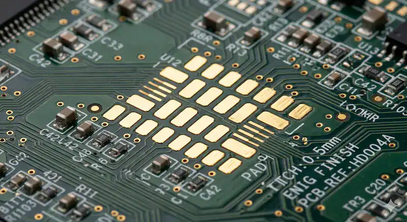
Electroless Nickel Immersion Gold serves as a premium two-layer metallic coating providing superior solderability for modern printed circuit boards. Many design engineers specify ENIG extensively because this process offers extraordinary oxidation resistance. Manufacturers require exceptionally flat contact areas for mounting complex semiconductor packages accurately. This chemical deposition method guarantees absolute uniform thickness across every exposed copper pad.
Core Layers Of The Finish
This specialized coating consists of two distinct functional metal layers working together seamlessly. An underlying nickel barrier blocks copper atoms from migrating upward into your final solder joint. A thin gold capping layer protects that nickel foundation from degrading before component placement occurs. Complex multi-layer designs rely heavily upon this specific dual-structure performance.
- Nickel thickness ranges from three up six micrometers generally.
- Gold depth stays between 1.6 and 2.8 microinches normally.
- Phosphorus integration dictates overall structural integrity.
Why Manufacturers Prefer It
Production facilities prefer this technique since it guarantees prolonged component shelf life. Circuit assemblies remain perfectly solderable even after twelve months sitting inside warehouse storage. Here is the deal. High-density interconnections demand perfectly planar surfaces which hot air solder leveling simply cannot provide. Exceptional pad flatness translates directly into higher first-pass assembly yields during mass production cycles.
Key Takeaway: Selecting this dual-layer protective strategy grants you flawless solderability alongside extended manufacturing windows.
| Layer Type | Primary Function | Standard Thickness |
|---|---|---|
| Electroless Nickel | Blocks copper diffusion | 3.0 – 6.0 µm |
| Immersion Gold | Prevents oxidation | 1.6 – 2.8 µin |
| Base Copper | Conducts electrical signals | Varies by design |
These specified deposition depths maintain an ideal balance between protection and cost efficiency.
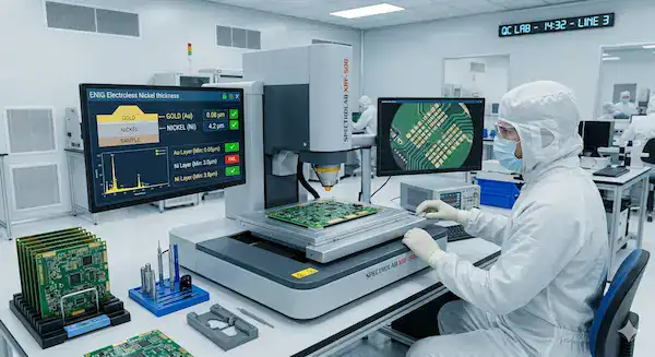
2. How Does The ENIG Plating Process Work Step By Step?
This complex plating process works through sequential chemical reactions involving rigorous cleaning, precise micro-etching, and controlled metal deposition stages. Every factory must monitor these acidic baths continuously so chemical concentrations remain perfectly balanced. We once received defective boards from another vendor running their nickel bath past recommended operating cycles. Phosphorus drifted up towards 14 percent causing massive BGA joint brittle fractures during thermal cycling tests. We now require every incoming ENIG lot include an XRF thickness report alongside nickel certification and we haven’t seen this failure over 18 continuous months.
Preparing The Copper Surface
Engineers begin by running bare copper panels through alkaline cleaning solutions removing oils and debris. Next comes a micro-etching step which slightly roughens metallic surfaces promoting superior mechanical adhesion. Unclean copper surfaces reject subsequent metallic plating attempts entirely causing disastrous cosmetic defects.
- Alkaline cleaners dissolve organic handling residues.
- Micro-etchants strip away native copper oxides.
- Pre-dip chemicals prepare panels for palladium activation.
Depositing Nickel And Gold
Palladium seeds act like catalytic anchors drawing nickel ions onto exposed copper features automatically. What does this mean for you? After building a solid nickel foundation, parts enter an immersion gold bath where a replacement reaction occurs. Gold atoms displace surface nickel atoms creating an ultra-thin protective noble metal barrier. Exact immersion timing dictates your final gold thickness accurately.
Key Takeaway: Tight chemical controls during each sequential bath dipping stage dictate final solder joint reliability.
| Process Step | Chemical Action | Quality Target |
|---|---|---|
| Micro-etching | Surface roughening | Uniform copper topography |
| Palladium Activation | Seeding catalyst | Complete pad coverage |
| Immersion Gold | Displacement reaction | Oxidation prevention |
Maintaining precise bath temperatures guarantees consistent metal deposition rates across entire production panels.
3. What Are The Key Advantages Of ENIG Over Other Finishes?
Primary benefits involve exceptional surface flatness alongside excellent oxidation resistance compared against traditional HASL processes. Incorporating ENIG protocols naturally allows manufacturers achieve highly dependable performance metrics regarding high-density interconnects. Standard hot air solder leveling creates uneven metallic domes which cause fine-pitch components great difficulty during placement operations. Electroless gold deposition establishes perfectly planar mounting pads accommodating even microscopic ball grid arrays perfectly.
Supreme Surface Flatness
Modern electronics demand increasingly miniaturized packaging formats possessing incredibly tight spacing tolerances. Coplanarity issues rapidly generate disastrous tombstoning defects when utilizing older uneven coating technologies. Perfectly flat pads prevent misaligned components during automated pick-and-place manufacturing sequences.
- Flat pads accommodate miniaturized passive components effortlessly.
- Planar surfaces support successful ball grid array attachment.
- Uniform plating depths prevent component misalignment anomalies.
Long Shelf Life Expectations
Untreated copper oxidizes swiftly upon exposure towards regular atmospheric moisture conditions. Applying noble metal barriers completely halts such destructive oxidation reactions effectively. You might be wondering. How long do these protected boards last inside standard storage facilities? Facilities routinely hold protected bare boards past twelve months without suffering any noticeable solderability degradation.
Key Takeaway: Exceptional pad flatness combined with extended storage capabilities makes this specific plating technique incredibly valuable.
| Advantage Category | Practical Production Benefit | Financial Impact |
|---|---|---|
| Surface Planarity | Zero component misalignment | Reduces rework expenses |
| Oxidation Resistance | Twelve month usable lifespan | Eliminates expired inventory |
| Wire Bonding | Supports aluminum wire attachment | Enables specialized packaging |
These listed benefits directly translate into higher factory throughput yields alongside decreased scrap material expenses.
4. ENIG Vs HASL: Which Surface Finish Should You Choose?
Choosing between these two distinct surface treatments depends heavily upon your specific component packaging requirements. Is paying extra processing costs justifiable when fabricating a basic two-layer prototype board? Many startups request HASL attempting upfront fabrication expense reductions. For a simple prototype utilizing standard 0603 passives alongside QFP-100 packages standard tin-lead leveling functions adequately. However, a recent client attempted using tin-lead leveling on mixed assemblies containing 0.4mm pitch parts. Uneven solder deposits caused a massive 35 percent rework rate during SMT operations. We instituted a firm engineering rule dictating any design possessing components below 0.5mm pitch automatically requires ENIG saving our partners thousands regarding hidden repair fees.
Cost Differences Explained
Traditional hot air leveling represents a significantly cheaper process requiring fewer chemical processing steps. Premium dual-layer plating commands higher initial purchase prices due towards expensive raw material requirements. Smart purchasing managers calculate total ownership costs before finalizing any vendor agreements.
- Two-layer boards exhibit larger percentage price gaps.
- Multilayer high-density designs shrink this relative cost difference.
- Total ownership costs must factor potential assembly repair fees.
Addressing Fine Pitch Needs
Components possessing pad spacing below half a millimeter strictly require perfectly flat landing zones. Listen closely. Attempting fine-pitch assembly operations across lumpy HASL topography guarantees disastrous manufacturing outcomes. You must evaluate total project expenses including anticipated defect rates rather than comparing bare board quotes alone. Selecting appropriate finishes upfront saves enormous debugging time later.
Key Takeaway: Select standard leveling techniques for simple designs while mandating premium chemical plating regarding advanced miniaturized products.
| Feature Metric | Hot Air Solder Leveling | Electroless Gold Plating |
|---|---|---|
| Coplanarity | Poor and uneven | Excellent and flat |
| Pitch Limit | Above 0.5 millimeters | Below 0.4 millimeters |
| Relative Cost | Very economical | Moderate premium |
Selecting appropriate coating technologies based upon component complexity dramatically improves final manufacturing success rates.
5. What Is ENIG Black Pad And How Can You Prevent It?
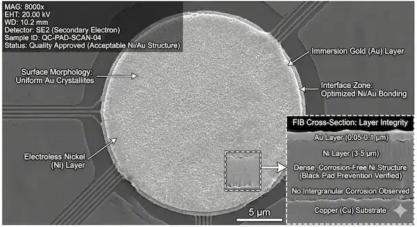
Black pad describes a catastrophic defect where hyper-corrosion destroys nickel layers beneath their protective gold caps. This destructive phenomenon generates extremely brittle solder joints which frequently fracture during thermal cycling stress tests. Root causes typically involve uncontrolled chemical baths driving phosphorus concentrations well beyond safe operational limits. Adding ENIG specifications lacking strict IPC compliance language leaves your supply chain vulnerable against these hidden flaws.
Root Causes Of Brittle Joints
Excessive immersion dwell times force acidic gold solutions deep into underlying nickel structures aggressively. This excessive galvanic corrosion strips away nickel atoms while leaving behind a structurally weak phosphorus-rich mud. Think about it. Dark oxidized nickel surfaces completely repel molten solder creating intermittent electrical connections.
- Nickel bath chemical imbalance accelerates unwanted corrosion reactions.
- Phosphorus levels exceeding 11 percent create brittle interfaces automatically.
- Multiple reflow passes dissolve healthy nickel continuously.
Effective Prevention Methods
Preventing these failures requires mandating strict adherence towards established international quality standards. Your fabrication partner must monitor chemical tank pH parameters continuously using automated dispensing systems. Requesting regular X-Ray Fluorescence thickness reports verifies that manufacturers deposit correct metal volumes consistently. Robust incoming quality inspections catch these microscopic defects before assembly begins.
Key Takeaway: Demanding verifiable chemical bath monitoring logs protects your sensitive products against devastating hidden joint fractures.
| Defect Trigger | Chemical Consequence | Prevention Strategy |
|---|---|---|
| Extended Gold Dwell | Excessive nickel corrosion | Limit immersion times strictly |
| High Phosphorus | Brittle intermetallic formation | Monitor bath turnover cycles |
| Thick Gold Plating | Galvanic attack acceleration | Cap thickness at 2.8 µin |
Proactive quality documentation reviews represent your best defense against catastrophic brittle fracture anomalies occurring post-assembly.
6. What Does IPC-4552 Specify For ENIG Quality And Thickness?
IPC-4552B specifies strict performance requirements regulating electroless gold deposition processes across commercial printed circuit manufacturing. This updated specification introduces detailed product rating systems evaluating corrosion severity utilizing precise statistical methodologies. Early document versions allowed slightly thicker gold deposits which inadvertently promoted aggressive nickel layer degradation. The revised standard tightly restricts maximum allowable gold depths while demanding rigorous visual cross-section inspections. Factories cannot simply rely upon basic thickness measurements anymore without performing detailed microscopic structural evaluations on their ENIG lines.
Updated Thickness Standards
Engineers formulated these tightened numerical limits specifically targeting hyper-corrosion defect mechanisms directly. Acceptable gold plating depths now sit comfortably between 1.6 and 2.8 microinches permanently. Maintaining exact chemical temperatures prevents rapid abnormal metal crystallization completely.
- Thinner gold caps minimize destructive galvanic driving forces.
- Nickel deposits must measure precisely between three and six micrometers.
- XRF measurement tools require frequent standardized calibration routines.
Corrosion Level Assessments
The newest revision mandates classifying any observed nickel attack into three distinct severity levels. Level three classifications automatically trigger full production lot rejections regardless regarding measured metal thickness values. Pay attention here. Inspectors must examine seven separate through-hole locations or five specific surface mount pads generating statistically valid assessments.
Key Takeaway: Enforcing these modern international standards guarantees your fabricated boards possess structurally sound metallic foundations.
| Inspection Parameter | IPC-4552A Standard | IPC-4552B Revision |
|---|---|---|
| Maximum Gold Depth | Up towards 5.0 µin | Strictly capped at 2.8 µin |
| Corrosion Check | Basic visual inspection | Product Rating System |
| Sample Size | Single random location | Seven specific defined points |
Transitioning towards these rigorous evaluation methodologies drastically reduces unexpected assembly line soldering failures.
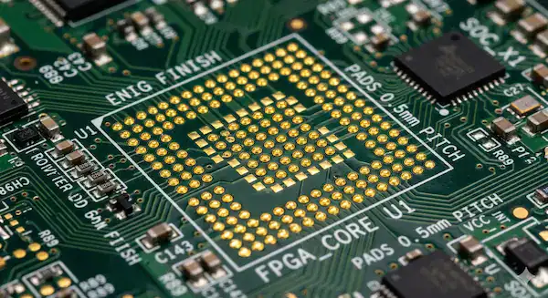
7. When Should You Use ENIG For Your PCB Design?
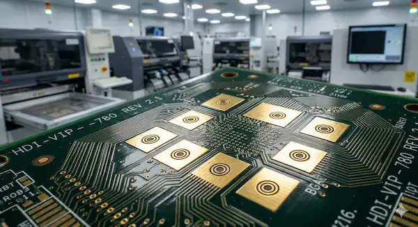
You should specify electroless gold coatings whenever routing architectures mandate tight tolerances alongside via-in-pad geometries. Using older organic preservatives across boards featuring via-in-pad structures frequently causes catastrophic capillary action problems. A medical equipment client tried utilizing organic solderability preservatives across designs featuring dense via-in-pad structures. Capillary action pulled molten alloy away from pads during reflow operations resulting in numerous open circuits. We immediately mandated ENIG over nickel coatings for all via-in-pad architecture moving forward. This single manufacturing adjustment completely eliminated via-related soldering defects across five subsequent large-scale production runs.
Via-In-Pad Requirements
Modern high-density routing frequently places conductive vias directly underneath ball grid array component pads. Applying traditional molten solder leveling over these open holes creates uneven bumps rendering flat component attachment impossible. Unfilled vias trap dangerous acidic chemical residues causing massive reliability failures eventually.
- Gold plating maintains perfectly planar surfaces above filled vias.
- Immersion silver alternatives often promote severe solder wicking phenomena.
- Flat pads guarantee proper spherical solder ball collapse during reflow.
Handling Tight Tolerances
Miniaturized semiconductor packages possessing 0.4 millimeter pin spacing require flawless coplanarity characteristics. This changes everything. Only chemical deposition processes offer sufficient precision matching these extreme mechanical dimensional constraints accurately. Premium finishes eliminate complicated soldering rework saving enormous engineering resources annually.
Key Takeaway: Complex routing topologies combined alongside dense component packaging necessitate premium chemical surface treatments absolutely.
| Design Feature | Recommended Finish | Technical Reasoning |
|---|---|---|
| Via-In-Pad | Electroless Gold | Prevents capillary solder wicking |
| 0.4mm BGA | Electroless Gold | Requires supreme pad coplanarity |
| Standard DIP | Hot Air Leveling | Tolerates uneven pad topographies |
Matching your chosen surface treatment against specific architectural routing complexities prevents disastrous assembly line bottlenecks.
8. How Does ENIG Compare To ENEPIG And Other Alternatives?
Electroless Nickel Electroless Palladium Immersion Gold adds a thin palladium barrier preventing aggressive nickel corrosion entirely. Operating radio frequency boards at frequencies exceeding 10GHz frequently exposes signal degradation problems stemming from magnetic nickel. High frequency signal transmission travels exclusively along outer conductor surfaces due towards established skin effect physics. Ferromagnetic nickel materials introduce measurable insertion losses degrading sensitive microwave communication signals significantly. While standard ENIG works wonderfully below 3GHz, higher frequency applications demand specialized non-magnetic alternative coatings.
Signal Integrity At High Frequencies
Engineers must evaluate potential signal attenuation whenever designing advanced telecommunication equipment running at extreme microwave bandwidths. Bare copper provides excellent conductivity but requires protection utilizing advanced organic preservatives lacking any magnetic properties. Selecting optimal finishes requires balancing performance metrics against raw material expenditures constantly.
- Nickel layers increase resistance against high-frequency alternating currents.
- ENEPIG utilizes thinner nickel deposits reducing total magnetic interference.
- Organic preservatives offer absolute minimum signal insertion loss profiles.
Choosing Based On Application
Projects requiring direct wire bonding procedures benefit immensely from palladium-fortified surface treatments. ENEPIG supports both aluminum and gold wire attachment methods flawlessly without suffering from black pad vulnerabilities. Let us dig deeper. You must balance increased palladium raw material costs against specific electrical performance demands carefully. ENEPIG represents ultimate versatility albeit demanding premium purchasing budgets entirely.
Key Takeaway: Reserve expensive palladium-fortified finishes strictly for specialized wire-bonding projects or highly sensitive microwave frequency applications.
| Surface Treatment | Magnetic Properties | Wire Bonding Capability |
|---|---|---|
| Standard ENIG | Highly ferromagnetic | Aluminum wire only |
| Premium ENEPIG | Low magnetic impact | Gold and Aluminum wire |
| Organic OSP | Non-magnetic entirely | Not supported whatsoever |
Selecting non-magnetic protective coatings preserves delicate radio frequency signal integrity across advanced microwave telecommunication products.
9. What Common ENIG Defects Should You Watch For?
Common defects you must avoid include skip plating phenomena alongside premature nickel layer oxidation before gold immersion. Contaminated chemical baths frequently cause uneven metal deposition leaving microscopic exposed copper regions completely unprotected. Integrating proper ENIG handling protocols eliminates localized contamination issues stemming from careless human interaction. Skin oils transferred via bare hands quickly degrade sensitive metallic surfaces ruining future solder wetting characteristics. Operators must wear clean protective gloves constantly whenever handling these unprotected printed circuit panels.
Identifying Nickel Oxidation
Delays occurring between nickel deposition and gold immersion stages invite rapid atmospheric oxygen contamination. Oxidized nickel surfaces repel gold replacement reactions creating visible dark spots scattered across mounting pads. Make no mistake. Strict timing protocols prevent these disastrous atmospheric exposure windows entirely.
- Dark patches indicate failed gold displacement reactions.
- Oxidized regions refuse molten solder wetting completely.
- Strict timing controls between chemical baths prevent oxygen exposure.
Managing Gold Plating Skips
Skip plating happens when trapped air bubbles block chemical fluids from touching specific copper geometries. Aggressive mechanical agitation inside plating tanks dislodges these microscopic gas bubbles successfully. This is where it gets interesting. Active fluid circulation systems maintain fresh chemical concentrations near every single dense routing feature. Vibrating racks shake stubborn bubbles loose verifying complete metallic coverage completely.
Key Takeaway: Rigorous facility cleanliness combined with automated material handling dramatically reduces cosmetic and functional plating defects.
| Defect Type | Visual Appearance | Primary Root Cause |
|---|---|---|
| Skip Plating | Exposed bare copper | Trapped air bubbles |
| Nickel Oxidation | Dark unplated patches | Process timing delays |
| Hand Contamination | Fingerprint shaped stains | Missing protective gloves |
Implementing strict environmental controls prevents these common contamination issues from ruining expensive fabricated circuit boards.
10. How To Evaluate Your Supplier’s ENIG Process Quality?
Verifying your supplier involves demanding detailed documentation proving strict adherence towards established international chemical processing standards. We audit dozens of raw material suppliers annually evaluating chemical bath management practices vigorously. One prospective vendor offered pricing 15 percent below current market averages recently. During our onsite facility audit, we discovered they routinely skipped daily X-Ray Fluorescence calibrations while failing basic corrosion assessments. We immediately disqualified them from our approved vendor list permanently. We strictly enforce routine SEM cross-section analysis alongside wetting balance tests across every vendor ENIG lot guaranteeing your final assemblies never fail due compromised plating.
Essential Documentation Checks
Professional fabrication houses maintain extensive daily logs recording chemical concentrations across every active production tank. You should request recent XRF measurement capability studies verifying their thickness metrology equipment functions accurately. Maintaining precise documentation separates legitimate factory operations from unreliable brokers immediately.
- Request documented IPC-4552B compliance certificates routinely.
- Review historical phosphorus concentration trending charts.
- Verify automated chemical dosing system calibration records.
Asking The Right Process Questions
Challenge prospective manufacturing partners regarding their specific metal bath turnover frequency schedules directly. Facilities stretching chemical lifespans artificially generate massive profitability margins while sacrificing your product reliability entirely. Here is your strategy. Ask them specifically how they execute Level Three corrosion assessments during routine quality control inspections. Honest technical responses prove genuine manufacturing expertise unconditionally.
Key Takeaway: Thorough auditing procedures separate dedicated professional manufacturers from dangerous corner-cutting discount fabrication shops effectively.
| Verification Method | Target Metric | Quality Indication |
|---|---|---|
| XRF Reporting | 1.6 – 2.8 µin gold | Proves thickness compliance |
| Chemical Logs | 7% – 11% phosphorus | Prevents brittle joints |
| Cross-section SEM | Zero hyper-corrosion | Confirms structural integrity |
Demanding transparent quality control documentation establishes a reliable foundation protecting your critical electronic hardware investments.
Reviewing these manufacturing facts reveals that selecting appropriate surface treatments dramatically influences final manufacturing yields. You must strictly enforce chemical bath monitoring while demanding rigorous thickness documentation from your fabrication partners. Prioritizing quality control metrics over initial purchase savings helps your engineering teams avoid devastating joint fractures successfully. If you demand reliable printed circuit solutions built upon proven engineering excellence, contact us today. Our engineering-driven agile manufacturing pipeline delivers transparent, data-driven manufacturing excellence protecting your brand reputation effortlessly.
FAQ
Q1: Can I use this finish for flexible circuits? Yes, you absolutely can utilize this coating upon flexible substrates. The thin metallic layers endure moderate bending stress without cracking making it highly suitable for polyimide-based flex applications.
Q2: How do I know if my board suffers from black pad? You must perform destructive cross-section analysis under a scanning electron microscope. This advanced imaging technique reveals dark oxidized nickel bands hiding beneath the top gold layer.
Q3: What’s the best way to store these finished boards? You should seal all bare panels inside moisture barrier bags containing active desiccant packs. Maintaining low humidity environments prevents moisture from attacking microscopic pores within the metal coating.
Q4: Can I rework a damaged gold pad? No, you cannot repair or re-plate individual damaged mounting pads successfully. Chemical deposition constitutes an irreversible batch process meaning compromised boards require complete replacement rather than localized repair.
Q5: How do I choose between this process and immersion silver? You should select gold plating when designs feature fine-pitch components requiring maximum shelf life. Choose silver alternatives only when seeking lower costs on simpler designs lacking via-in-pad geometries.