
Quick Answer: When comparing a 6 layer vs 8 layer pcb, the 8-layer upgrade typically adds 30% to 50% to your bare board costs, but it becomes an absolute requirement for signals exceeding 10Gbps. For prototypes (10 pcs), 8 layers run $200–$400 compared to $150–$300 for 6 layers, while mass production (500+ units) shrinks that gap to just a $2–$10 difference per board.
Key takeaways:
- DDR4 and PCIe Gen3 route reliably on an optimized 6-layer design.
- DDR5 (4800MT/s+) and PCIe Gen4+ strictly require 8 layers to pass emissions.
- A custom dual-ground 6-layer stackup saves 25–30% while handling up to 10Gbps.
- Spending an extra $500 on 8-layer prototypes prevents $5,000+ in failed EMC testing fees.
Table of Contents
- What Is the Real Structural Difference Between a 6-Layer and 8-Layer PCB?
- Which Stackup Arrangement Actually Matters for Signal Integrity?
- Can a 6-Layer PCB Handle DDR4 or DDR5 Memory Routing?
- How Much Does Upgrading from 6 to 8 Layers Actually Cost?
- What Is the Best 6-Layer Stackup If You Can’t Afford 8 Layers?
- When Is 8 Layers Non-Negotiable — and When Is It Overkill?
- How Does Layer Count Affect Your PCB Manufacturing Lead Time?
- FAQ
You’ve hit a routing wall, and your signal integrity simulations are flashing red warnings. The temptation is to stick with a cheaper board, but the hidden risk of a failed EMC test looms over your project timeline. After processing over 2,400+ assembly orders last year, we’ve seen startups burn thousands of dollars guessing on the 6 layer vs 8 layer pcb decision. Here is the engineering data to determine exactly when you can save money with a smarter 6-layer layout, and when paying for 8 layers is the only way your product survives certification.
What Is the Real Structural Difference Between a 6-Layer and 8-Layer PCB?
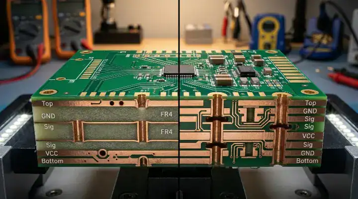
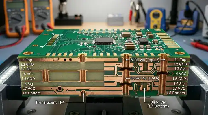
The fundamental structural difference between a 6-layer and an 8-layer PCB is the return path isolation; 8 layers provide every high-speed signal layer with its own dedicated, adjacent ground plane, while standard 6-layer boards force two signal layers to share a single reference. This added isolation in 8-layer boards reduces crosstalk by up to 40% and provides significantly more physical routing space for tight BGA breakouts.
But here’s what most guides won’t tell you… the layer count alone means nothing without looking at the core and prepreg arrangement.
As a multilayer PCB manufacturer, we constantly see designers moving up from a 2-layer vs 4-layer PCB directly into 6 or 8 layers without understanding the structural shifts:
- Standard 6-Layer Risk: Typically configured as Sig/GND/Sig/Sig/PWR/Sig. Layers 3 and 4 sit adjacent to each other without a plane between them, creating massive broadside crosstalk if you run parallel traces.
- Standard 8-Layer Advantage: Configured as Sig/GND/Sig/GND/PWR/Sig/GND/Sig. Every single internal routing layer is tightly coupled to a solid ground or power plane.
- Manufacturing Yield: 8-layer boards demand tighter layer-to-layer registration and higher drilling accuracy, which slightly lowers the raw factory yield compared to standard 6-layer builds.
| Feature | Standard 6-Layer PCB | Standard 8-Layer PCB |
|---|---|---|
| Stackup Structure | Sig/GND/Sig/Sig/PWR/Sig | Sig/GND/Sig/GND/PWR/Sig/GND/Sig |
| Signal Integrity | Good for < 5Gbps | Excellent up to 25Gbps+ |
| EMI Shielding | Moderate (Shared return paths) | High (Dedicated return paths) |
| Routing Density | Medium (BGA pitch > 0.8mm) | High (BGA pitch < 0.8mm) |
| Prototype Cost (10pcs) | $150 – $300 | $200 – $400 |
| Volume Cost (500pcs) | $8 – $25 per board | $10 – $35 per board |
Which Stackup Arrangement Actually Matters for Signal Integrity?
For signal integrity, the thickness of the dielectric between your signal trace and its immediate reference plane dictates your impedance stability far more than the total board thickness. A perfectly executed 6-layer stackup maintains a stable 50-ohm single-ended impedance, but an 8-layer stackup physically separates analog noise from digital high-speed lines using dedicated shielding layers.
The real question is… are you actually using your layers correctly?
We see a massive oversight in how hardware startups handle layer assignments. Last year, 80% of the RF IoT boards we received using standard 6-layer stackups failed their initial impedance software checks due to poorly specified prepreg thickness. We mandate an automated stackup review that adjusts copper weight and prepreg before fabrication, dropping our customers’ impedance failure rate from 18% to under 0.5%.
To get this right from day one, you must:
- Route high-speed traces strictly adjacent to continuous GND planes.
- Avoid routing critical signals over split planes or gaps.
- Use a proper PCB stack-up design guide to define your trace widths before you place a single component.
Upload your Gerber files to our portal for a free DFM engineering review to verify your impedance targets are actually manufacturable.
Can a 6-Layer PCB Handle DDR4 or DDR5 Memory Routing?

A 6-layer PCB reliably handles DDR3 and DDR4 routing up to 3200 MT/s if your BGA pitch is at least 0.8mm, your signal traces remain under 75mm, and you use a modified dual-ground stackup. However, attempting to route DDR5 at 4800MT/s or higher on 6 layers carries extreme timing risks and strictly requires an 8-layer board to manage the tight jitter tolerances.
Want the honest answer? We see this exact debate constantly on hardware engineering forums regarding iMX6 processor boards. Startup engineers want to save money on 6 layers, but memory routing is unforgiving.
If you are using DDR3 or DDR4, you do not need 8 layers. You can execute this perfectly on 6 layers by abandoning the default stackup. Instead of the standard configuration, you must use Sig/GND/Sig/GND/PWR/Sig. This gives your address and data buses a solid reference.
If you are working with DDR5, the margins for error simply vanish. Forcing DDR5 onto 6 layers demands incredibly dense stitching vias and flawless length matching that most budget CAD tools cannot simulate accurately. If budget permits, upgrade to 8 layers.
| Interface Type | Signal Speed | Recommended PCB Layers | Factory Reasoning |
|---|---|---|---|
| USB 2.0 / 3.0 | 480 Mbps / 5 Gbps | 6 Layers (Optimized) | Return paths easily managed with standard trace spacing. |
| PCIe Gen 1-3 | Up to 8 GT/s | 6 Layers (Optimized) | Tolerates minor impedance variations; 6 layers work well. |
| DDR3 / DDR4 | < 3200 MT/s | 6 Layers (Optimized) | 0.8mm BGA allows escape routing; lengths stay short. |
| PCIe Gen 4 / 5 | 16 GT/s – 32 GT/s | 8 Layers | Requires absolute signal isolation and dedicated GND. |
| DDR5 / LPDDR5 | 4800+ MT/s | 8 Layers | Tight jitter budgets; zero tolerance for crosstalk. |
| 100G Ethernet | 25 Gbps per lane | 8 Layers | PAM4 signaling requires ultra-stable return paths. |
How Much Does Upgrading from 6 to 8 Layers Actually Cost?
Upgrading from a 6 layer vs 8 layer pcb adds approximately $500 to $1,500 for a prototype run of 10 boards, but that price gap shrinks drastically to just $10 to $35 per board for mass production runs of 500 units. Making this layer count decision during the initial schematic phase saves 90% of the redesign costs compared to adding layers after your first prototype fails.
So what does this actually mean for your budget? Hardware engineers frequently ask if the prototype cost bump is worth it. Let’s look at the actual ROI. If you force a dense design onto 6 layers and it fails FCC or CE emissions testing due to EMI leakage, the lab re-certification fees range from $3,000 to $8,000.
By calculating your total PCB fabrication cost correctly:
- The Trap: Saving $150 on prototype bare boards.
- The Consequence: Spending $5,000 on failed EMI testing, plus two weeks rewriting the layout.
- The Fix: Spend the extra $150 upfront on 8 layers.
If your signal speeds breach that 10Gbps barrier, the 8-layer premium is an insurance policy against multi-thousand dollar delays. Get a transparent quote within 24 hours from our team to see the exact price delta for your specific BOM.
What Is the Best 6-Layer Stackup If You Can’t Afford 8 Layers?
The best 6-layer stackup for high-speed design abandons the standard layout for a dual-ground configuration: Signal / Ground / Signal / Ground / Power / Signal. This configuration mimics 8-layer performance for signals under 10Gbps by providing adjacent return paths for the most critical routing layers, saving you 25% to 30% in fabrication costs.
Here’s where it gets real… startups operating on a tight MVP budget cannot always justify 8 layers.
To make this 6-layer optimized stackup work, you must actively manage the transition points where signals jump between layers. Because you do not have infinite ground planes, you must calculate and place stitching vias near your signal vias to provide a return path for the high-frequency current.
Use this specific spacing formula based on your highest frequency:
- For 1 GHz signals: Place stitching vias with a spacing of < 30mm.
- For 3 GHz signals: Place stitching vias with a spacing of < 10mm.
Understand the hard limit here: this 6-layer optimization works brilliantly for industrial controllers and mid-speed digital boards. However, the moment your signals cross 10Gbps, this workaround degrades. Do not push a 6-layer board past its physical physics threshold.
When Is 8 Layers Non-Negotiable — and When Is It Overkill?
An 8-layer PCB is non-negotiable when routing signals faster than 16GT/s, such as PCIe Gen 4, or when designing densely packed boards with a BGA pitch below 0.65mm that require microvias. Conversely, paying for 8 layers is a total waste of capital if your maximum frequency sits below 500MHz and you have plenty of physical routing space on the outer layers.
Now, here’s the part that surprises most customers… more layers do not automatically equal a better product.
If you are a startup building a simple motor controller or a standard IoT sensor node, strong component placement fixes 90% of your routing problems. If your board meets the “Overkill” criteria below, stick to 6 layers. If you hit the “Mandatory” triggers, particularly those requiring HDI PCB manufacturing techniques, 8 layers are required.
| Scenario | Choose 6 Layers (Optimized) | Upgrade to 8 Layers (Mandatory) |
|---|---|---|
| Signal Speeds | Under 10 Gbps | Over 10 Gbps (PCIe Gen4, DDR5) |
| Component Density | BGA pitch ≥ 0.8mm | BGA pitch ≤ 0.65mm |
| RF / Mixed Signal | Simple sub-1GHz radios | Complex multi-radio + sensitive analog |
| Power Requirements | Single main voltage rail | Multiple high-current rails requiring planes |
| Project Stage | Budget-restricted MVP | Mission-critical aerospace or medical device |
How Does Layer Count Affect Your PCB Manufacturing Lead Time?

Fabricating an 8-layer board typically takes 1 to 2 days longer than a 6-layer board because the factory must execute an additional pressing cycle and maintain tighter alignment tolerances. While standard 6-layer boards can occasionally be rushed in 48 hours, reliable 8-layer production generally requires a minimum 5-day lead time.
That said… pushing a factory to rush a complex multilayer board introduces risk.
For 8-layer boards, the lamination process requires precise temperature and pressure profiling to prevent delamination. Furthermore, the aspect ratio of the drilled vias becomes more challenging as the board thickness increases. We utilize 3D AOI and X-Ray inspection on every BGA joint regardless of layer count, but 8-layer boards require more meticulous setup time on the factory floor.
Plan your production schedule assuming a 5-to-7 day turn for 8-layer prototypes to guarantee perfect registration.
FAQ
Can I use blind and buried vias on a 6-layer board? Yes, you can, but it defeats the cost-saving purpose. Adding blind or buried vias requires multiple lamination cycles, which immediately makes your 6-layer board more expensive than a standard through-hole 8-layer board. Stick to standard through-hole vias on 6 layers to keep costs low. Upload your Gerber files today to compare standard vs HDI manufacturing costs.
Will moving to 8 layers automatically fix my EMI problems? No, it will not. An 8-layer board provides the physical planes needed for good EMI shielding, but if you route traces over split planes or fail to place decoupling capacitors correctly, you will still fail emissions testing. Layer count enables good design; it does not replace it. Request a free DFM engineering review on your layout to catch EMI risks early.
How do I know if my BGA component requires 8 layers? It depends entirely on the pin pitch and the pin count. If your BGA has a 0.8mm pitch, you can usually escape route it on a 6-layer board. If the pitch drops to 0.65mm or 0.5mm with hundreds of pins, there is physically not enough room on the internal layers to fan out the traces without upgrading to an 8-layer HDI structure. Contact our engineering team to review your exact BGA footprint.
Written by the QueenEMS Engineering Team. Ready to build your next board? Contact us today at QueenEMS.