
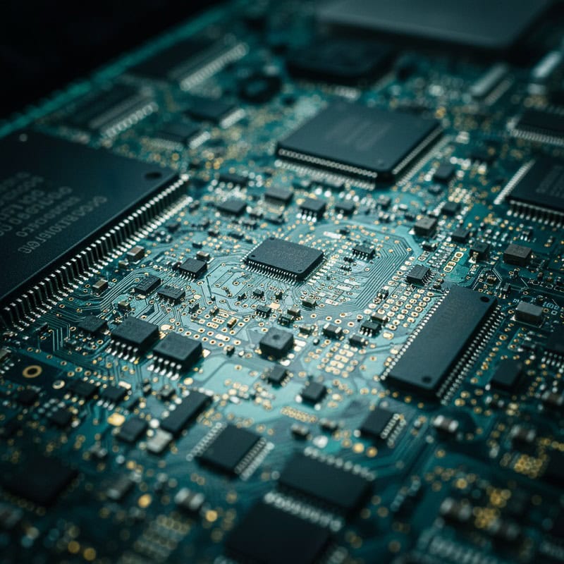
What is the significance of high-speed PCB design for modern artificial intelligence hardware? Many hardware engineers struggle with signal degradation and thermal management when developing high-performance computing platforms. Failing to address these complexities leads to system instability and expensive hardware recalls. We provide high-end PCB solutions with advanced DFM expertise to ensure your AI infrastructure remains robust and scalable. Here is the deal. This guide offers a technical analysis of the structural and material requirements for the next generation of artificial intelligence hardware.
1. What is the significance of continuous ground planes in high-speed design?
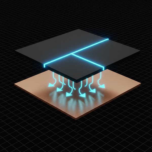
A continuous ground plane serves as the foundational reference for high-speed signals by providing a low-impedance return path. When you route traces over a broken or split plane, the return current must find a longer path, creating a large loop area that increases electromagnetic interference. You might be wondering how this affects the signal integrity of an AI server board. In dense 28-layer designs, even a small gap in the reference plane can cause significant impedance discontinuities. This leads to reflections that distort the digital pulse, especially at data rates exceeding 56Gbps. By maintaining a solid plane, you effectively shield the signal and maintain the tight impedance control required for BGA Assembly of high-pin-count processors. The continuity of the plane acts as a barrier against crosstalk from adjacent layers, ensuring that sensitive data lines are isolated from power switching noise. Engineers must prioritize layer stackup planning to ensure that every high-speed signal layer has at least one adjacent, uninterrupted ground plane.
| Frequency Range | Recommended Plane Strategy | Impact on Signal Integrity |
| < 100 MHz | Single reference plane is often sufficient | Low risk of EMI issues |
| 100 MHz – 1 GHz | Dedicated ground layers adjacent to signal layers | Improved return path control |
| 1-10 GHz | Continuous ground planes with high-Dk materials | Significant reduction in crosstalk |
| > 10 GHz | Multiple ground planes with back-drilled vias | Essential for PAM4 signal clarity |
2. How to optimize via placement for 28-layer AI server boards?

Improperly placed vias create areas with increased current density, which can lead to localized heating and potential delamination. What’s the real story? When you cluster vias too closely together, they effectively act as a physical barrier to the power planes, choking the current flow. This is particularly dangerous for AI accelerators that demand hundreds of amps. The best method involves positioning vias in a precise grid pattern, ensuring enough space for power and ground planes to pass through without interruption. Using a grid-pattern distribution ensures that the thermal load is spread evenly across the 28 layers of the PCB stackup. This approach is a cornerstone of our SMT Assembly process, ensuring that every via contributes to a stable and reliable power delivery network. Furthermore, optimizing the anti-pad size around these vias is crucial to minimize the capacitance and inductance that could otherwise distort high-frequency signals at the transition point between layers.
| Placement Pattern | Current Density Distribution | Impact on Thermal Management |
| Random Clustering | Highly Uneven | High risk of hot spots |
| Staggered Pattern | Moderate Uniformity | Better heat dissipation |
| Grid Pattern | Highly Uniform | Optimal for high-power AI chips |
| Honeycomb Pattern | Superior Uniformity | Maximum space for power planes |
3. Why should you avoid 90-degree trace bends in 112G PAM4 signals?
High-speed signals are incredibly sensitive to any change in the geometry of the transmission line. Wait, there’s more. A 90-degree bend creates a wider corner where the trace width effectively changes, leading to a sudden drop in impedance. At 112G PAM4 speeds, this discontinuity causes reflections that can ruin the eye diagram of the signal. It is recommended to use 135-degree bends or even rounded corners to minimize these reflections. By keeping bends to a minimum and using obtuse angles, you ensure that the signal energy remains focused along the path. This level of precision is exactly what we provide during our PCB Prototyping and Quick Turn services to validate your high-speed designs before mass production. Beyond impedance issues, sharp corners can also cause manufacturing defects such as acid traps during the etching process, leading to long-term reliability concerns in high-stress data center environments.
| Bend Type | Impedance Discontinuity | Reflection Loss at 28GHz | Recommendation |
| 90-Degree Sharp | High | Significant | Avoid entirely |
| 135-Degree Mitered | Low | Minimal | Standard for high-speed |
| Rounded Corner | Very Low | Negligible | Best for 112G+ signals |
| S-Curve | Variable | Depends on Radius | Used for length matching |
4. How can increased trace spacing mitigate crosstalk in dense layouts?
Crosstalk occurs when the electromagnetic field from one trace couples into an adjacent trace, causing unwanted noise. This is where it gets interesting. The level of crosstalk depends heavily on the spacing between traces and the length over which they run parallel. A common rule is to maintain a minimum spacing of four times the trace width (4W) between adjacent signals in the same net. In areas where routing becomes tight, designers often create bottlenecks where spacing is reduced. In such situations, the spacing should be immediately increased as soon as the signal exits the narrow area. Maintaining this distance is vital for Mixed Assembly projects where sensitive analog signals must coexist with noisy digital high-speed lines. Implementing vertical isolation through ground planes between signal layers can also drastically reduce broadside crosstalk, allowing for higher density without sacrificing data integrity or signal clarity in AI-driven workloads.
| Spacing Rule | Crosstalk Reduction | Typical Application |
| 2W Spacing | Minimal | Low-speed digital logic |
| 3W Spacing | Moderate | Standard high-speed (10Gbps) |
| 4W Spacing | High | Advanced AI server signals |
| 5W+ Spacing | Maximum | Critical clock and timing lines |
5. What is the impact of long stubs on signal integrity at high frequencies?
Long stubs act as unintended antennas that can radiate energy or create severe signal reflections. Ready for the good part? When a signal reaches a stub, part of the energy travels down the stub and reflects back, interfering with the main signal path. This interference creates “dips” in the frequency response, known as resonance points. To prevent this, signals should be routed in a closed loop or the stubs should be eliminated entirely through techniques like back-drilling. Managing these parasitic elements is a critical part of the Hardware Startups journey, as early-stage designs often overlook these high-frequency nuances. Using proper topology instead of long stubs ensures that your AI hardware passes electromagnetic compatibility (EMC) testing on the first try. Designers should also consider blind and buried vias to effectively manage layer transitions without leaving residual copper stubs that could compromise the channel bandwidth in next-generation PCIe 6.0 architectures.
| Stub Type | Signal Frequency | Resonance Effect | Recommended Solution |
| Through-hole via | < 5 GHz | Low | Standard manufacturing |
| Internal layer stub | 10-25 GHz | Moderate | Blind/Buried vias |
| Long via stub | 56-112 GHz | Severe | Mandatory Back-drilling |
| Blind microvia | > 112 GHz | Negligible | HDI Stackup |
6. How to achieve perfect symmetry in differential pair routing?
Differential signals must be kept at a consistent distance and routed symmetrically to maintain specified differential impedance. Think about it. If one trace of a differential pair is longer than the other, the signals will arrive at the receiver at different times, causing common-mode noise. Designers should avoid placing any components or vias between the differential pairs, even if the routing appears symmetrical. Doing so creates impedance discontinuities that can lead to EMC issues. Both traces of a differential pair should always be routed on the same layer to ensure they experience the same environmental conditions. This level of care is standard in our Consumer Electronics production lines to guarantee high-quality signal transmission. Precise length matching is equally important, as even a small mismatch can cause phase shift errors that distort high-speed PAM4 eyes beyond recovery.
7. Why is back-drilling essential for high-speed AI hardware?
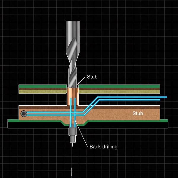
In a multi-layer board, a via typically passes through all layers, but the signal may only need to travel from the top to an internal layer. What’s the catch? The remaining portion of the via, known as the stub, creates a significant impedance mismatch. For AI servers operating at 56G or 112G, these stubs must be removed via back-drilling to prevent signal degradation. Back-drilling uses a larger drill bit to remove the copper plating from the unused portion of the via. This process is vital for applications like Industry Automation where sensors and controllers must communicate with extreme precision and speed. Reducing the stub length to under 10 mils effectively moves the resonance point outside the frequency band of interest, preserving the integrity of high-speed digital transitions and reducing overall jitter in the system.
| Stub Length | Max Usable Frequency | Impact on Signal Eye |
| > 40 mils | < 5 GHz | Severe closure of eye diagram |
| 15 – 40 mils | 5 – 15 GHz | Moderate jitter and noise |
| 5 – 15 mils | 15 – 30 GHz | Clean eye for PCIe Gen 5 |
| < 5 mils | > 30 GHz | Optimal for 112G/224G PAM4 |
8. How to handle split planes without compromising return paths?
A signal should never be routed across a split plane because the return path cannot follow the signal trace. But here’s the kicker. If a return path is forced to find a long way around a split, the area between the forward and return paths behaves like a loop antenna. This results in massive noise coupling and EMI problems that can fail regulatory certifications. If a signal must cross two different reference planes, decoupling capacitors should be used to provide a bridge for the return current. This technique allows the return current to pass from one reference plane to another with minimal impedance. Such solutions are frequently implemented in our Telecommunications projects to ensure network stability. For ultra-high-speed lines, designers should entirely avoid split plane crossings by rearranging the stackup or trace paths to maintain 100% reference plane coverage.
9. What are the best practices for separating analog and digital grounds?
To minimize noise in mixed-signal circuits, it is standard practice to separate analog and digital ground planes. You might be wondering how to connect them without creating a ground loop. The ideal method is to connect both planes at a single point, usually near the main integrated circuit, using a ferrite bead or a zero-ohm resistor. This prevents digital switching noise from polluting the sensitive analog environment. In mixed-signal designs with split planes, you must never route a digital signal across the analog ground plane. This separation is especially critical in Medical PCB Assembly where signal precision can be a matter of life and death. Furthermore, keeping digital high-speed traces away from the boundary of the analog section ensures that radiated emissions do not couple into sensitive low-voltage sensors or diagnostic circuits.
10. How to match trace width to component size for optimal impedance?
Matching trace width to the physical size of the component pads is essential for reducing reflections at the interface. Now we’re getting somewhere. Sudden changes in trace width lead to impedance tuning issues that can disrupt high-speed signal performance. Designers must carefully adjust the trace width as it enters the component pad to ensure a smooth transition. This is particularly challenging for high-density components like 0.4mm pitch BGAs. Our expertise in Robotics PCB fabrication ensures that these fine-pitch components are integrated with the highest level of signal integrity. Using tapered trace transitions or teardrops can provide a more gradual change in impedance, effectively dampening the reflections that occur when high-speed signals hit large component pads or via landing rings.
Conclusion
High-speed PCB design for AI infrastructure requires a meticulous balance of signal integrity, thermal management, and precision manufacturing. By following these 10 advanced tips, engineers can ensure that their hardware remains stable under the extreme demands of modern computing. Ready to take the next step? We recommend collaborating with an experienced manufacturing partner who understands these complexities. Our team is ready to support your next project from initial prototyping to full-scale production.
Final Thoughts
The rapid evolution of artificial intelligence is pushing the limits of traditional PCB fabrication. Prioritizing advanced techniques like back-drilling and mSAP is no longer optional for high-performance systems. Leverage our state-of-the-art About facility and technical expertise to bring your vision to life.
FAQ Section
Q1: What is high-speed PCB design?
High-speed PCB design refers to creating circuit boards where signal integrity is significantly affected by the physical characteristics of the board, such as layout and materials, due to the high frequencies and rapid rise times of the signals.
Q2: How does back-drilling work?
Back-drilling involves using a specialized CNC machine to drill out the unused copper portion of a plated through-hole via, which reduces unintended signal reflections and improves high-frequency performance by removing via stubs.
Q3: Why is impedance control important?
Consistent impedance ensures that signals travel from the source to the receiver without reflecting off discontinuities, which is essential for maintaining data integrity and reducing jitter in high-speed digital circuits.
Q4: When should I use HDI technology?
HDI should be used when component pin pitches are so small that traditional routing cannot accommodate the required number of connections, or when you need to significantly reduce the physical size and layer count of the board.
Q5: What are the benefits of mSAP?
The Modified Semi-Additive Process (mSAP) allows for much finer trace widths and more precise vertical sidewall geometries than traditional subtractive etching, which is vital for maintaining impedance accuracy in 112G+ high-speed signal paths.