
Making sense of wave soldering means understanding how a cascading pan of molten solder perfectly secures thousands of through-hole components to a printed circuit board simultaneously. You spend weeks meticulously laying out a dense mixed-technology board, only to suffer massive bridging and cold joints during mass production because the thermal profiles were completely misaligned. This frustrating yield drop severely ruins your delivery schedule and dramatically inflates your internal engineering rework costs. By mastering the wave soldering process and applying strict DFM rules, you can completely eliminate these defects and guarantee a flawless, high-speed assembly run every single time.
Contents
- What exactly is the wave soldering process?
- How does the 4-step wave soldering workflow operate?
- What are the optimal wave soldering machine flux types?
- How do wave soldering thermal profiles prevent damage?
- Why use laminar and turbulent wave soldering dynamics?
- What are the pros and cons of wave soldering techniques?
- How does wave soldering vs reflow vs selective compare?
- Which lead-free wave soldering alloys perform best?
- How to design for wave soldering using DFM rules?
- How do you troubleshoot common wave soldering defects?
What exactly is the wave soldering process?
The wave soldering process is an automated mass-soldering technique where a circuit board passes over a precisely controlled, cascading pan of molten solder. Engineers rely on this highly efficient industrial methodology to securely attach traditional through-hole components and specific surface-mount devices to the bottom layer of complex electronic assemblies. A continuously pumping impeller drives the liquid alloy upward to create a standing wave that thoroughly washes over the exposed metallic pads and component leads. The surface tension of the molten metal combined with capillary action pulls the liquid alloy up into the plated through-holes to form flawless, permanent electro-mechanical bonds.
How did this mass production process evolve?
Early electronics manufacturing relied almost entirely on incredibly slow, labor-intensive manual hand-soldering techniques that severely bottlenecked production throughput during the golden age of vacuum tubes. As consumer demand for televisions and radios exploded globally, engineers developed the first automated drag-soldering machines to submerge entire board bottoms into massive liquid solder baths. Modern continuous wave technologies subsequently emerged to eliminate the severe oxide accumulation problems associated with static solder pots by constantly recycling fresh, highly active liquid metal. Today, advanced manufacturing facilities utilize heavily computerized, nitrogen-inerted systems that drastically reduce dross formation while accommodating highly complex, multi-layered mixed-technology electronic architectures flawlessly.
What are the core mechanical principles involved?
The foundational physics driving this manufacturing method center entirely on controlling fluid dynamics, thermal transfer rates, and precise metallurgical wetting reactions within incredibly tight processing windows. Here is the deal: The conveyor system must maintain an absolutely perfect inclination angle to allow excess liquid solder to effortlessly peel away from the receding circuit board surface.
- The impeller pump controls wave height and fluid velocity.
- The conveyor angle prevents massive solder bridging defects.
- The flux chemistry chemically strips away interfering oxides.
| Development Era | Primary Soldering Method | Manufacturing Throughput |
|---|---|---|
| Early 1950s | Manual hand soldering | Extremely low volume |
| 1960s – 1980s | Static drag soldering | Moderate batch processing |
| 1990s – Present | Computerized dual wave | Ultra-high mass production |
This historical progression table clearly illustrates how relentless industrial automation continuously transformed agonizingly slow manual labor into incredibly efficient, high-speed electronic manufacturing capabilities.
Key Takeaway: You must deeply understand the fundamental fluid dynamics and historical context of this machinery because optimizing your modern production yields fundamentally requires respecting these uncompromising physical metallurgical principles.
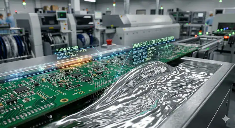
How does the 4-step wave soldering workflow operate?
The 4-step wave soldering workflow operates through a rigidly controlled, continuous sequence consisting of flux application, intense preheating, direct liquid wave contact, and accelerated cooling. Every single printed circuit board traveling down the automated conveyor belt must seamlessly pass through these four distinct operational zones without experiencing any sudden interruptions or jarring vibrations. If any individual stage within this highly integrated mechanical sequence drifts out of its specified tolerance window, the final assembled product will inevitably suffer from catastrophic electrical connectivity failures. You must continuously monitor and rigorously calibrate each sequential processing zone to ensure the entire electronic assembly successfully survives the extreme thermal shock of mass soldering.
What happens during fluxing and preheating?
The process initiates when specialized nozzles spray a carefully measured chemical flux layer across the bottom surface to aggressively strip away invisible oxidation from the copper pads. Immediately afterward, the circuit board enters an intense preheating tunnel where powerful infrared heaters rapidly elevate the overall substrate temperature to safely evaporate the volatile flux solvents. This critical thermal ramping phase physically prepares the delicate fiberglass matrix and sensitive electronic components to absorb the impending thermal shock of the molten metal wave. Picture this: Skipping the preheat stage traps volatile liquids inside the plated holes, causing explosive outgassing that violently ejects liquid solder during the subsequent wave contact phase.
How do wave contact and cooling function?
The preheated board subsequently slides perfectly over the crest of the molten solder wave, allowing capillary forces to aggressively suck the liquid alloy deep into the component via holes. Following this brief liquid contact, heavy-duty cooling fans immediately blast the exiting substrate with high-velocity air to rapidly solidify the molten joints into robust, permanent connections.
- Flux application removes oxidation chemically.
- Preheating prevents catastrophic thermal shock.
- Wave contact creates the metallurgical bond.
- Cooling solidifies the liquid solder instantly.
| Workflow Stage | Primary Function | Failure Consequence |
|---|---|---|
| Flux Application | Oxide removal | Cold, non-wetting joints |
| Board Preheating | Solvent evaporation | Explosive blow holes |
| Wave Contact | Solder deposition | Insufficient via fill |
| Rapid Cooling | Joint solidification | Grainy, fractured joints |
This comprehensive workflow matrix highlights exactly how a single failure in any sequential processing zone cascades into severe, unrecoverable metallurgical defects during the final manufacturing phase.
Key Takeaway: You must rigorously calibrate your machine to smoothly transition boards between these four critical stages because abrupt thermal or mechanical shifts guarantee catastrophic soldering defects.
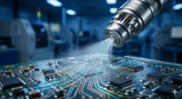
What are the optimal wave soldering machine flux types?
The optimal wave soldering machine flux types include traditional rosin-based, aggressive water-soluble, and modern no-clean chemical formulations depending entirely on your specific end-use reliability requirements. Choosing the correct chemical activation agent dictates how successfully the molten liquid alloy will wet the exposed copper surfaces while simultaneously preventing aggressive long-term dendritic growth. You must perfectly match your chosen flux chemistry to your specific cleaning capabilities, as highly corrosive residues left behind on the board will inevitably destroy sensitive signal traces. Carefully evaluating your overall manufacturing environment and customer cleanliness specifications ultimately determines which specific flux chemical formulation will maximize your production yield rates safely.
How do corrosive and no-clean fluxes differ?
Water-soluble fluxes utilize highly aggressive organic acids that provide absolutely exceptional metallurgical wetting characteristics but mandate immediate, vigorous aqueous washing to prevent catastrophic post-production corrosion. Conversely, modern no-clean formulations utilize very mild organic compounds designed to safely burn off during the preheating phase, leaving behind a benign, electrically invisible residue. While no-clean fluxes save immense amounts of money by completely eliminating the expensive post-soldering wash cycle, they struggle significantly to clean heavily oxidized, older component leads. Now let’s get down to business: You cannot safely use aggressive water-soluble chemistries if your complex board design features unsealed mechanical relays that might trap corrosive washing fluids.
What are the best application methods?
Modern manufacturing facilities almost exclusively utilize precision ultrasonic spray fluxing systems because they deposit an incredibly uniform, micron-thin layer of chemicals precisely where required. Older foam fluxing methodologies bubble compressed air through a porous stone to generate a chemical froth, but this messy technique frequently clogs and applies excessive, wasteful volumes.
- Spray fluxing minimizes chemical consumption waste.
- Foam fluxing handles deep through-hole penetration.
- Drop-jet fluxing targets specific component areas.
| Flux Chemistry | Activity Level | Post-Soldering Cleaning |
|---|---|---|
| Rosin Mildly Activated | Low to Medium | Solvent wash recommended |
| Water-Soluble Organic | Extremely High | Mandatory hot water wash |
| Low-Solids No-Clean | Very Low | No cleaning required |
This chemical comparison table vividly illustrates the fundamental engineering tradeoff between achieving superior metallurgical wetting characteristics and managing expensive post-production circuit board cleaning requirements.
Engineers frequently report yield drops after switching from water-soluble to no-clean flux because they fail to adjust two critical parameters simultaneously. First, no-clean flux has significantly lower activation energy, so you must increase your preheat top-side temperature by 10–15°C to fully activate the milder organic acids. Second, your incoming bare board surface finish matters far more with no-clean chemistry. OSP finishes older than 6 months develop invisible oxide layers that water-soluble flux can power through but no-clean formulations cannot. The practical solution is to tighten your incoming material shelf-life controls to a maximum of 3 months for OSP boards when using no-clean flux, or switch to an ENIG surface finish that resists oxidation indefinitely.
Key Takeaway: Always select a low-solids no-clean flux formulation whenever possible to drastically reduce your overall manufacturing costs, provided your incoming bare boards remain completely oxidation-free.
How do wave soldering thermal profiles prevent damage?
Wave soldering thermal profiles prevent damage by carefully ramping up the overall board temperatures to chemically activate the flux without causing severe mechanical thermal shock. A perfectly engineered thermal gradient ensures the heavy copper planes expand at a manageable rate, preventing the delicate plated through-holes from violently tearing themselves apart. You must meticulously attach highly sensitive thermal couples directly to a sacrificial test board to accurately measure the precise heat absorption rates across various densely populated zones. Failing to adequately measure and continuously adjust these extreme thermal parameters practically guarantees your expensive electronic components will suffer from invisible, irreversible heat-induced internal stress fractures.
Why is preheating absolutely critical for survival?
The intense preheating tunnel performs the absolutely vital task of safely boiling away the volatile alcohol solvents suspended within the liquid flux before the board hits the wave. If these volatile liquids survive the preheat zone, they will violently vaporize upon contacting the 260°C molten solder, creating explosive blow holes that ruin the connection. Truth be told: Thick, multi-layered industrial backplanes require significantly longer, heavily sustained preheating durations compared to thin consumer boards just to achieve the same optimal top-side temperatures.
What are the exact thermal parameters required?
Engineers must rigidly adhere to strict metallurgical guidelines dictating maximum ramp rates, exact peak wave temperatures, and highly controlled post-solder cooling velocities for different alloys. Standard lead-free alloys absolutely require substantially higher peak operating temperatures and significantly tighter processing windows compared to traditional legacy eutectic lead-based manufacturing materials.
- Keep preheat ramp rates below 2°C per second.
- Maintain top-side preheat temperatures around 100°C.
- Limit wave contact time to exactly 3-5 seconds.
| Thermal Parameter | Traditional Leaded (Sn63Pb37) | Modern Lead-Free (SAC305) |
|---|---|---|
| Top-Side Preheat Temp | 85°C to 105°C | 110°C to 130°C |
| Peak Wave Temperature | 240°C to 250°C | 255°C to 270°C |
| Maximum Contact Time | 3.0 to 4.0 seconds | 4.0 to 5.0 seconds |
| Ideal Cooling Ramp Rate | < 2.0°C per second | < 3.0°C per second |
This exact thermal profiling table definitively proves that modern RoHS-compliant manufacturing demands significantly more aggressive heating strategies that push electronic components dangerously close to their absolute survival limits.
Key Takeaway: You must physically run a fully instrumented thermal profiler board through your specific machine at the start of every shift to guarantee your thermal gradients remain perfectly within specification.
Why use laminar and turbulent wave soldering dynamics?
You use laminar and turbulent wave soldering dynamics in a dual-wave system to ensure complete joint penetration while simultaneously wiping away excess liquid solder bridges. Modern high-density circuit boards heavily populated with miniature surface-mount devices glued to the bottom side completely disrupt the smooth flow of a single, traditional flat wave. You fundamentally require the aggressive, chaotic scrubbing action of a turbulent primary wave to force liquid metal into the tight, shadowed crevices hidden behind bulky components. Following this chaotic application, the board immediately slides over a perfectly smooth, glassy laminar wave that gracefully pulls away excess solder to create flawlessly formed, professional fillets.
When should you engage the turbulent chip wave?
You must engage the chaotic primary turbulent wave whenever your circuit design features bottom-side surface-mount components, such as tiny ceramic capacitors or discrete resistor networks. The turbulent fluid dynamics physically disrupt the invisible insulating pockets of outgassing flux vapors that naturally form behind component bodies as they rapidly plow through the liquid metal. Believe it or not: Trying to solder densely packed bottom-side components using only a smooth laminar wave guarantees massive skip defects because the liquid solder simply cannot penetrate the shadowing effect.
How does the laminar wave finish the joint?
The secondary laminar wave provides a perfectly flat, highly controlled liquid mirror surface that gently sweeps across the entire board bottom to refine the metallurgical bonds. It functions precisely as an active thermal squeegee, melting away the massive ugly solder globs deposited by the turbulent wave and pulling the excess material back into the pot.
- Turbulent waves scrub away vapor pockets aggressively.
- Laminar waves shape the final solder fillet perfectly.
- Dual systems prevent both skips and massive bridging.
| Wave Dynamics | Fluid Characteristics | Primary Defect Prevented |
|---|---|---|
| Single Laminar | Smooth, glassy, slow flow | Best for bridging on simple boards |
| Primary Turbulent | Chaotic, high-pressure jet | Eliminates shadowing skips |
| Secondary Laminar | Flat, controlled wiping action | Removes excess solder webs |
This fluid dynamics breakdown illustrates why a modern dual-wave machine architecture remains absolutely essential for successfully processing highly complex, mixed-technology electronic assemblies without suffering from rampant short circuits.
Key Takeaway: Always activate both the turbulent and laminar impellers when processing boards featuring glued bottom-side components to ensure perfectly wetted joints without suffering from catastrophic solder bridging.
What are the pros and cons of wave soldering techniques?
The pros and cons of wave soldering techniques involve massive production speed advantages weighed heavily against significantly higher material waste and complex mechanical setup requirements. This robust industrial process remains the undisputed champion for churning out thousands of heavy-duty power supplies and industrial control boards featuring massive, heat-sucking through-hole connectors. However, the requirement to maintain a massive, constantly heated pot containing hundreds of pounds of expensive liquid alloy makes this technique incredibly cost-prohibitive for small, low-volume prototype runs. You must carefully calculate your anticipated manufacturing volumes and specific component layouts before committing expensive factory floor space to this massive, energy-hungry continuous processing equipment.
What are the primary manufacturing benefits?
The absolute greatest advantage of this continuous mass-soldering methodology is its unparalleled ability to securely attach thousands of disparate through-hole components in mere seconds. Once the engineering team perfectly dials in the precise thermal profile and conveyor speed, the machine can blindly process hundreds of massive circuit boards per hour flawlessly. You might be wondering: This exceptional throughput speed drastically lowers the per-board manufacturing labor cost compared to utilizing dozens of highly trained technicians performing slow manual hand-soldering operations.
Where does the continuous process fall short?
The system notoriously consumes massive amounts of electrical power to keep the massive solder pot molten, and it continuously burns off expensive alloy as useless surface dross. Furthermore, the chaotic fluid dynamics simply cannot handle ultra-fine-pitch modern surface mount components, severely limiting its applicability for modern, highly miniaturized smartphone or wearable electronic architectures.
- Exceptional high-volume production speeds.
- Outstanding metallurgical through-hole penetration.
- Massive energy and alloy material consumption.
| Production Factor | Identified Advantage | Inherent Limitation |
|---|---|---|
| Processing Speed | Thousands of joints per second | Long initial machine setup times |
| Operational Cost | Lowest cost for mass production | High standby energy consumption |
| Component Focus | Perfect for bulky through-hole | Destroys fine-pitch SMD parts |
This honest manufacturing capability matrix clearly defines why this legendary technology remains dominant for heavy industrial electronics while slowly disappearing from ultra-compact consumer mobile device assembly lines.
Key Takeaway: You should fiercely leverage this exceptionally fast technology for high-volume power electronics, but strictly avoid it when designing highly miniaturized boards featuring extremely tight, fine-pitch surface-mount components.
How does wave soldering vs reflow vs selective compare?
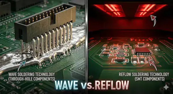
The comparison of wave soldering vs reflow vs selective reveals profound technical differences in application scope, heavy equipment costs, and ultimate processing throughput speeds. Reflow ovens utilize precisely heated ambient air to gently melt pre-printed solder paste for delicate surface-mount devices without ever exposing the entire board to a terrifying liquid metal bath. Selective soldering employs a tiny, robotically controlled miniature solder fountain to meticulously pinpoint individual through-hole pins without thermally disturbing the surrounding, highly sensitive miniature SMD components. You must understand how these three distinct manufacturing technologies perfectly complement each other to successfully build complex, modern mixed-technology products without compromising overall structural reliability.
When is reflow the vastly superior option?
Reflow manufacturing absolutely dominates the modern electronics landscape because it perfectly accommodates the microscopic, high-density surface-mount chips driving today’s advanced mobile and computing technologies safely. It relies on extremely precise stencils to deposit microscopic bricks of solder paste, allowing the gentle infrared oven heat to gracefully pull components into perfect alignment via surface tension. Let’s dive in: You simply cannot use a liquid wave to attach a massive BGA processor because the chaotic fluid would instantly short out all the hidden microscopic pads underneath.
Why choose selective systems for complex boards?
Selective robotic systems perfectly bridge the gap by safely processing bulky through-hole connectors on double-sided boards where a traditional massive liquid wave would instantly destroy the bottom-side surface-mount parts. While significantly slower than traditional mass-soldering, selective machines drastically reduce expensive masking tape labor and completely eliminate the massive alloy dross waste associated with giant, continuously pumping solder pots.
- Reflow handles massive volumes of tiny SMDs safely.
- Traditional waves process massive through-hole volumes quickly.
- Selective robotics handle complex mixed-tech precisely.
| Process Technology | Ideal Component Type | Production Speed | Defect Rate Risk |
|---|---|---|---|
| Reflow Soldering | Fine-pitch SMD & BGAs | Extremely Fast | Very Low (If pasted correctly) |
| Wave Soldering | Bulky Through-Hole | Very Fast | High (If poorly designed) |
| Selective Soldering | Mixed-Tech Through-Hole | Moderately Slow | Extremely Low |
This comprehensive tri-technology comparison table demonstrates exactly how modern factories intelligently deploy different thermal processing machines to safely construct highly complex boards featuring vastly different component packaging styles.
This is one of the most common questions from engineers designing their first mixed-technology board. Yes, you can wave solder bottom-side SMD components, but only passive chip parts (0603 and larger) and simple SOT-23 packages. You must first secure these components with red epoxy adhesive dots, cure the adhesive at approximately 150°C in a dedicated oven, and then run the board through the wave. Components must be oriented with their pads parallel to the wave travel direction to prevent shadowing. Critical restrictions apply: you cannot wave solder QFN, BGA, or any package with solder pads hidden underneath the body. Fine-pitch ICs (0.5mm pitch and below) also cannot survive the chaotic wave dynamics. For boards with these components on the bottom side, selective soldering is your only automated option. The general industry rule is: if your bottom-side has only passives and simple discretes, wave soldering with glue works well at high volumes; if you have any IC packages on the bottom, invest in selective soldering.
Key Takeaway: You must strategically design your electronic assemblies knowing exactly which specific soldering machine will process each side of the board to prevent impossible, un-manufacturable component layouts.
Which lead-free wave soldering alloys perform best?
The lead-free wave soldering alloys that perform best are SAC305 and SN100C due to their excellent metallurgical wetting characteristics and total compliance with strict international RoHS environmental regulations. Choosing the correct liquid alloy chemistry fundamentally dictates the mechanical shock resistance, the required operating temperatures, and the overall physical appearance of the final solidified solder joint fillets. Since the global electronics industry aggressively banned toxic lead, manufacturers have struggled with higher melting temperatures that ruthlessly attack expensive copper traces and rapidly dissolve the machine’s internal steel pumping mechanisms. You must carefully balance the extremely high raw material costs of silver-infused alloys against the superior, shiny cosmetic finish provided by trace additions of nickel and germanium.
Why has the industry abandoned Sn63Pb37?
For decades, the legendary Sn63Pb37 eutectic lead alloy reigned supreme because it melted at a beautifully low 183°C, flowed like water, and created incredibly robust, ultra-shiny joints effortlessly. However, heavy metal toxicity concerns and strict European environmental legislation permanently banned its use in consumer goods, forcing engineers to adopt highly abrasive, high-temperature tin-based alternatives. This is where it gets interesting: These modern alternatives stubbornly refuse to wet oxidized copper easily and frequently leave behind dull, grainy-looking joints that constantly trigger false alarms during visual quality inspections.
How do modern lead-free alternatives stack up?
The SAC305 alloy, featuring tin, silver, and copper, provides fantastic mechanical strength but costs an absolute fortune due to fluctuating global silver commodity market prices. Conversely, the brilliant SN100C formulation eliminates the expensive silver entirely, relying instead on trace amounts of nickel to generate beautifully smooth, shiny joints that incredibly closely mimic traditional leaded aesthetics.
- SAC305 delivers exceptional mechanical drop-shock resistance.
- SN100C provides a much cheaper, highly cosmetic shiny finish.
- High-tin alloys aggressively dissolve the copper pads.
| Alloy Specification | Composition Elements | Melting Point | Wetting Ability | Relative Cost |
|---|---|---|---|---|
| Sn63Pb37 (Legacy) | 63% Tin, 37% Lead | 183°C | Perfect | Very Low |
| SAC305 (RoHS) | 96.5% Sn, 3% Ag, 0.5% Cu | 217°C | Moderate | Extremely High |
| SN100C (RoHS) | 99.3% Sn, 0.7% Cu, +Ni/Ge | 227°C | Good | Medium |
This metallurgical specification table reveals that while modern eco-friendly alloys effectively protect the environment, they fundamentally force manufacturers to tolerate significantly higher melting temperatures and substantially increased raw material expenditures.
Nitrogen inerting delivers measurable, documented improvements that directly impact your bottom line. In lead-free wave soldering, nitrogen reduces dross formation by 50–80% compared to air atmosphere, which alone can save $500–$2,000 per month in alloy waste depending on pot size. More importantly, nitrogen dramatically improves wetting performance of high-tin lead-free alloys by preventing the rapid surface oxidation that causes bridging and cold joints. Real-world production data consistently shows a 15–25% reduction in overall defect rates when switching from air to nitrogen for SAC305 alloy processing. The investment typically pays for itself within 6–12 months through reduced alloy consumption and lower rework costs. However, nitrogen is not a substitute for proper flux selection and thermal profiling. If your process already suffers from fundamental parameter issues, adding nitrogen will only mask the symptoms temporarily.
Key Takeaway: You should specify the silver-free SN100C alloy for standard commercial electronic assemblies to significantly drastically reduce your raw material costs while simultaneously improving the final cosmetic appearance of the joints.
How to design for wave soldering using DFM rules?
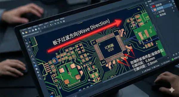
You design for wave soldering using strict DFM rules that aggressively dictate component orientation, precise pad spacing, and the exact board travel direction over the liquid metal. A brilliantly designed schematic completely falls apart on the factory floor if the physical layout prevents the molten alloy from easily accessing and smoothly exiting every single component pin. You must strategically orient all polarized components parallel to the machine’s conveyor direction to actively prevent taller component bodies from casting invisible metallurgical shadows over trailing pins. Failing to implement these critical geometric design guidelines absolutely guarantees your finished boards will suffer from rampant solder bridging and massive, unrecoverable skip defects during mass production.
How does component orientation affect yields?
When a bulky rectangular surface-mount component travels perpendicular to the liquid wave, the physical body brutally deflects the fluid flow, creating a massive dry pocket immediately behind it. This devastating shadowing effect physically prevents the liquid solder from ever touching the trailing pad, resulting in a completely open circuit that requires expensive, agonizing manual hand-soldering rework. Here is the deal: By simply rotating the component 90 degrees in your CAD software, both pads enter the liquid wave sequentially, guaranteeing perfect, flawless metallurgical wetting on every single connection.
What are the crucial rules for pad spacing?
Engineers must drastically increase the physical spacing between adjacent copper pads compared to standard reflow designs, as the massive volume of liquid metal desperately wants to bridge the gaps. You must employ specialized teardrop pad geometries and aggressive solder mask dams to physically block the liquid metal from crawling across the bare substrate to neighboring pins.
- Align all SMDs parallel to the wave direction securely.
- Add massive sacrificial solder thieves to trailing IC pins.
- Maximize the pitch spacing between adjacent through-hole leads.
| DFM Design Rule | Geometric Implementation | Primary Defect Prevented |
|---|---|---|
| Component Orientation | Align parallel to board travel | Shadowing & solder skips |
| Trailing Pad Thieves | Add dummy pads to rear of ICs | Massive trailing edge bridging |
| Pad Pitch Spacing | Increase gap > 2.0mm for wave | Inter-pin solder shorts |
This rigorous DFM rule table perfectly illustrates how proactive mechanical geometry adjustments executed deeply within the CAD software seamlessly eliminate massive physical manufacturing defects on the factory floor.
Key Takeaway: You must clearly indicate the intended machine travel direction directly on your silkscreen layer so the factory operator feeds the board perfectly aligned with your intended fluid dynamics strategy.
How do you troubleshoot common wave soldering defects?
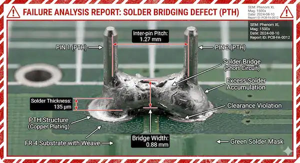
You troubleshoot common wave soldering defects by systematically isolating machine parameters like conveyor speed, chemical flux volume, and exact preheat temperatures to eliminate the root mechanical cause. When massive quality control failures suddenly halt your production line, you cannot simply guess at random machine adjustments; you must deeply analyze the physical characteristics of the failing joints. Every single metallurgical defect leaves behind highly specific visual clues indicating exactly whether the failure stems from catastrophic thermal shock, severe chemical contamination, or terrible fluid dynamic stripping. By meticulously documenting your machine settings and comparing the failures against known industry defect standards, you can rapidly restore your high-speed manufacturing line to perfect operational status.
Why do bridging and icicles randomly occur?
Solder bridging occurs when excessive liquid metal physically spans across two adjacent pins, typically caused by a conveyor belt running entirely too fast to allow proper fluid drain-off. Similarly, massive metallic icicles form pointing downward when the preheat temperature is dangerously low, causing the liquid alloy to freeze solid instantly before it can gracefully snap back into the pot. What is the real story? Both of these incredibly frustrating excess-solder defects directly indicate that your machine’s critical thermal gradients or fluid separation dynamics are completely out of acceptable tolerance.
How can you permanently fix skips and blow holes?
Solder skips happen when the liquid wave simply never touches the copper pad, usually demanding a massive increase in the primary turbulent impeller speed to aggressively scrub away protective vapor pockets. Explosive blow holes internally rupture the joint when trapped moisture boils violently; fixing this nightmare requires immediately baking the bare circuit boards in an oven before running them through the machine.
- Bridging requires slowing the conveyor for better drainage.
- Icicles demand significantly higher preheat and pot temperatures.
- Blow holes require pre-baking moisture out of the boards.
| Defect Name | Visual Characteristic | Root Cause | Effective Troubleshooting Fix |
|---|---|---|---|
| Solder Bridging | Metal shorting across pins | Conveyor too fast, bad flux | Slow conveyor, verify flux spray |
| Metal Icicles | Sharp spikes pointing down | Insufficient preheating temp | Increase top-side preheat temp |
| Solder Skips | Dry pads with zero solder | Wave shadowing, low turbulence | Increase primary turbulent wave |
| Blow Holes | Craters ruptured in the joint | Trapped moisture in the PCB | Pre-bake bare boards for 24 hours |
| Insufficient Fill | Solder doesn’t reach top | Conveyor too fast, low heat | Slow conveyor, increase contact time |
This comprehensive defect troubleshooting table acts as an absolutely essential survival guide for manufacturing engineers desperately fighting to restore acceptable yield rates during a chaotic mass-production crisis.
Solder ball formation during wave soldering has two primary root causes that engineers frequently confuse. The first is moisture-related outgassing: if your boards absorb humidity during storage, the trapped moisture flash-evaporates upon contacting the 260°C solder wave, violently ejecting tiny solder droplets onto the board surface. The solution is to bake boards at 120°C for 2–4 hours before wave soldering if they have been stored in uncontrolled humidity for more than 48 hours. The second cause is excessive or improperly applied flux. When the spray fluxer deposits too much flux or distributes it unevenly, the excess volatile solvents that survive the preheat zone will explode upon contacting the wave, creating identical solder ball scatter patterns. To diagnose which cause is responsible, run a test: bake a batch of boards thoroughly and run them through the wave. If solder balls disappear, the issue is moisture. If they persist, your flux application parameters need adjustment, specifically reducing the spray pressure and increasing preheat dwell time by 10–15 seconds.
Key Takeaway: Never adjust more than one machine parameter at a time when actively troubleshooting defects, otherwise you will permanently lose track of which specific mechanical variable actually solved the metallurgical failure.
Conclusion
This comprehensive guide resolved the immensely complex mechanical, thermal, and chemical challenges inherent to mass manufacturing, proving that proactive DFM geometry and precise thermal profiling are absolutely mandatory. By aggressively applying these strict troubleshooting techniques and optimizing your component layouts for fluid dynamics, you successfully eliminate catastrophic bridging defects and significantly accelerate your time to market. We deliver expert 2-hour quotations, rigorous engineering DFM reviews, and flawlessly executed high-speed assembly services to physically protect your vital production deadlines. To secure your next high-volume mixed-technology run with guaranteed engineering excellence, please contact us today and experience unmatched factory-direct precision.
FAQ
Q1: Can I use wave soldering for ultra-fine-pitch SMD components? No. The chaotic fluid dynamics and massive surface tension of the liquid metal wave will instantly bridge and destroy any surface-mount component with a pin pitch smaller than 0.65mm.
Q2: What’s the best way to prevent explosive blow holes during production? Baking your bare circuit boards in a low-temperature oven for 24 hours before assembly is the best method. This safely drives out all trapped ambient moisture that would otherwise violently boil when hitting the 260°C liquid alloy.
Q3: How do I know if I need a dual-wave or single-wave machine? Check your bottom-side component layout. If you have glued SMDs on the bottom layer, you absolutely require a dual-wave system (turbulent and laminar) to aggressively prevent shadowing skips behind the component bodies.
Q4: Can I run both leaded and lead-free boards in the exact same machine? No. You must never mix these alloys in the same pot, as cross-contamination legally violates RoHS environmental compliance and fundamentally destroys the mechanical integrity of the metallurgical joints.
Q5: What’s the best method to apply flux for high-density, complex boards? Precision ultrasonic spray fluxing is the absolute best method. It allows you to strictly control the exact micro-volume of chemicals applied, preventing messy, corrosive residues from becoming trapped inside sensitive mechanical relays or tight connectors.