
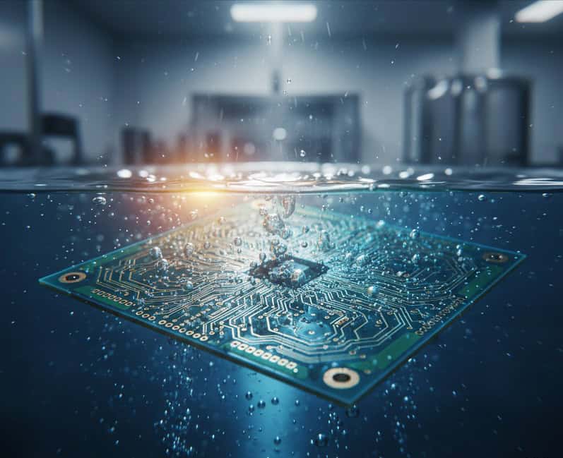
PCB Etching 101: Methods, Process Steps, and Best Practices provides the definitive roadmap for navigating the complex copper removal phase in modern electronics fabrication. What is pcb etching? Effectively, the pcb etching process involves chemically or physically removing unwanted copper layers from a substrate to reveal precise circuit patterns required for electrical functionality. Managing this stage remains a common headache for procurement managers because improper execution leads to catastrophic board failure and wasted budgets. But here’s the kicker… even the most advanced designs will fail if the etching isn’t handled by an expert partner who prioritizes precision over speed. At QueenEMS, we provide the solution by integrating state-of-the-art etching controls within our comprehensive manufacturing workflow to ensure your hardware reaches the market without defects. Our deep engineering background establishes the trust you need to scale production confidently from prototype to mass volume.
1. What is the fundamental role of pcb etching in manufacturing?
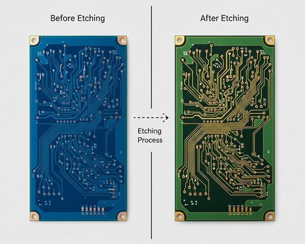
The pcb etching phase essentially acts as the “sculpting” stage of fabrication where the functional circuitry is finally born from a solid copper sheet. What’s the real story? While the design specifies where signals should travel, it is the etching process that physically creates these paths by dissolving excess metal. This step is indispensable because it determines the final impedance and conductivity of every trace on your board. Without a tightly controlled chemical environment, you risk losing the fine details that modern high-speed electronics absolutely require to function.
How does the etching process define circuit geometry?
The etching process removes all copper not protected by a resist layer, creating the conductive paths that link your components. ● Defining Traces: It sets the final width and thickness of the circuit tracks. ● Clearing Gaps: It ensures there is no residual copper between traces to prevent short circuits. ● Layer Formation: It is repeated for every layer in a multi-layer PCB stack-up.
You might be wondering how we maintain such tight tolerances on complex designs for our medical pcb assembly clients. We utilize specialized chemical resists that protect essential traces while the surrounding copper is washed away. For B2B clients, this means fewer scrapped boards and significantly higher production yields.
Key Takeaway
Precise etching is the foundation of electrical reliability; it ensures that your digital design translates perfectly into a physical, high-performance circuit board.
| Phase | Description | Impact |
| Imaging | Transferring the circuit pattern | Accuracy of layout |
| Etching | Removing excess copper | Trace integrity |
| Stripping | Removing protective resist | Final circuit quality |
2. How do you distinguish between wet and dry pcb etching methods?
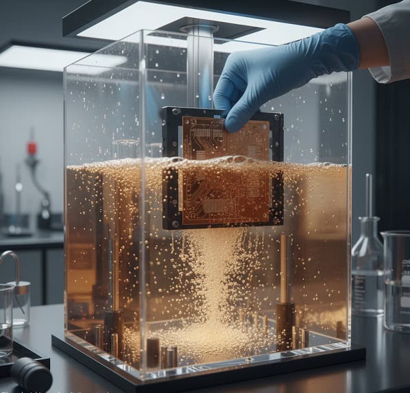
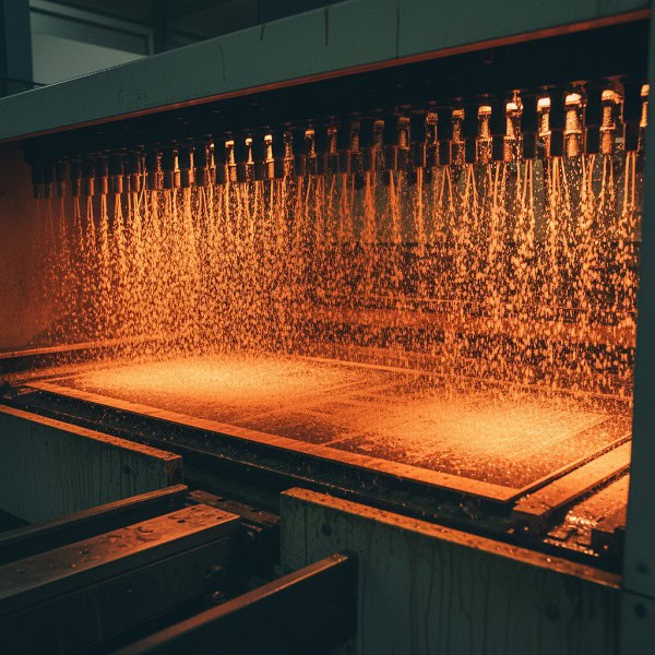
Distinguishing between wet and dry pcb etching methods requires understanding the trade-off between high-volume throughput and ultra-fine precision. Ready for the good part? Most standard consumer electronics projects utilize wet etching because it is remarkably fast and cost-effective for large batches. This method involves submerging panels in chemical baths or passing them through conveyorized spray chambers to dissolve copper. Dry etching, conversely, uses plasma or lasers to remove material without liquid chemicals, offering a level of precision that liquids cannot match.
Which method fits your production volume?
Choosing the right method is the first step in optimizing your manufacturing cost and performance. ● Wet Etching: Best for standard multi-layer boards and high-volume commercial orders. ● Dry Etching: Necessary for ultra-fine-line technology and military-grade precision. ● Laser Etching: Ideal for rapid prototyping without the need for chemical waste.
Here’s the deal: wet etching remains the workhorse of the industry because of its efficiency in removing large areas of copper quickly. However, dry etching is becoming more common as industry automation demands smaller and more integrated components. At QueenEMS, we evaluate your design to recommend the method that best balances your budget and performance needs.
Key Takeaway
Choosing the right method is about finding the sweet spot between manufacturing speed and the technical requirements of your circuit density.
| Method | Precision Level | Cost Efficiency | Typical Application |
| Wet Etching | 50-100 Microns | High | Commercial PCBs |
| Dry Etching | Sub-10 Microns | Low | High-density HDI |
3. Why is alkaline pcb etching the preferred choice for outer layers?
Alkaline pcb etching is the preferred choice for outer layers because it is highly compatible with the tin or lead-tin plating used as an etch resist. This is where it gets interesting… unlike acidic etchants, alkaline solutions do not attack the metallic plating that protects your circuitry. This allows us to etch the outer layers of a panel after the holes have been plated, ensuring a consistent electrical connection throughout the board. This chemical stability makes it the industry standard for complex telecom equipment and large-scale PCBA projects.
Why is ammonia-based chemistry so effective?
The ammonia-based solution maintains a stable pH that ensures the tin resist remains completely intact during the spray process. ● Tin Compatibility: It selectively removes copper without damaging the protective plating. ● High Etch Rate: The chemical reaction is fast, allowing for high-speed conveyor production. ● Standardization: It is the most widely documented and reliable process for outer layers.
What’s the real story? The speed of alkaline etching means the process must be perfectly timed to avoid “undercutting,” where the chemical eats away at the copper underneath the protective tin. Our engineers monitor these spray cycles with precision to ensure your traces remain robust for complex bga assembly.
Key Takeaway
Alkaline etching is a strategic choice for high-reliability sectors where consistent outer-layer connectivity is mandatory.
| Parameter | Range | Monitoring Method |
| pH Level | 8.0 – 8.8 | Automated Sensors |
| Temperature | 45°C – 55°C | Thermal Feedback |
| Copper Content | 120 – 160 g/L | Dosing Pump |
4. Can acidic pcb etching provide better precision for inner layers?
Acidic pcb etching provides superior precision for inner layers because it offers a more stable and predictable etch rate than alkaline alternatives. You might be wondering why we distinguish between layers; the answer is that inner layers do not have plated holes yet and use a photoresist rather than a metallic resist. This allows us to use cupric chloride or ferric chloride, which provides much cleaner vertical edges on your copper traces. For high-density medical pcb assembly projects, this precision is vital for signal integrity.
How does cupric chloride improve trace quality?
Using a stable acidic bath allows for cleaner vertical walls on your copper traces, which is vital for impedance control. ● Low Undercut: It minimizes lateral copper removal, keeping traces closer to the design width. ● Continuous Regeneration: The chemistry can be recycled in real-time, reducing environmental waste. ● Fine Line Capability: It supports the tight spacing required for high-density designs.
Here’s the deal: because acidic etching is so predictable, it allows designers to push the limits of trace density. By using this method, we can achieve the tight spacing required for modern, miniaturized electronics without risking copper slivers or shorts. This level of control is detailed in technical guides on soldering defects found on Wikipedia.
Key Takeaway
Acidic etching ensures that the hidden internal layers of your board are manufactured to the same exacting standards as the visible surfaces.
| Etchant | Precision | Ease of Use | Environment |
| Cupric Chloride | High | High | Recyclable |
| Ferric Chloride | Medium | Moderate | Disposal Required |
5. How does plasma pcb etching achieve ultra-fine precision?
Plasma pcb etching achieves ultra-fine precision by utilizing ionized gas in a vacuum chamber to “blast” away copper atoms at a microscopic level. Ready for the good part? This dry process eliminates surface tension issues that liquid chemicals face when trying to enter very small gaps in robotics boards. Plasma allows us to create traces that are far smaller than what traditional chemical etching could ever achieve. This makes it an essential tool for advanced aerospace applications where every millimeter of space counts.
What makes gas better than liquid?
Ionized plasma provides a highly directional (anisotropic) etch, meaning it only removes copper in a downward direction. ● Zero Undercut: It does not eat away at the copper underneath the resist. ● Cleanliness: No liquid residue is left in the micro-vias or deep holes. ● Material Diversity: It can etch through materials that are resistant to standard acids.
But here’s the kicker… while plasma is incredibly precise, it is much slower and more expensive than traditional wet etching. We typically reserve this method for bga assembly and other ultra-fine pitch technologies where reliability outweighs cost. Using plasma represents the cutting edge of the electronics industry as we push toward even smaller devices.
Key Takeaway
When your design requires traces smaller than the industry standard, plasma etching is the only way to guarantee electrical continuity.
| Feature | Plasma Etching | Chemical Etching |
| Medium | Ionized Gas | Liquid Acid/Base |
| Precision | Sub-micron | 50+ Microns |
| Undercut | Zero | 15-30% |
6. Is laser pcb etching the future of rapid prototyping?
Laser pcb etching represents a massive leap forward for speed because it eliminates the need for physical masks or chemical baths. What’s the real story? By using a high-powered beam to vaporize copper directly, we can go from a design file to a physical board in a fraction of the time. This makes it perfect for pcb prototyping and quick turn services where every hour matters for engineers. It is a cleaner, faster, and more flexible way to build the first versions of your hardware.
How does laser direct imaging (LDI) change the game?
Lasers provide a digital-to-physical workflow that is both cleaner and faster than traditional methods. ● Instant Iteration: You can change your circuit design and have a new board in minutes. ● No Chemicals: It is an environmentally friendly alternative to toxic etching baths. ● High Flexibility: It can etch complex patterns on flexible substrates for drone electronics.
You might be wondering if laser etching can handle mass production. While it is revolutionary for prototypes, the time required to “scan” a large panel with a laser beam makes it slower for huge orders. However, for small batches of specialized hardware, it is an unbeatable solution.
Key Takeaway
Laser etching is the ultimate tool for rapid iteration, allowing you to test and refine your hardware designs in days rather than weeks.
| Factor | Laser Etching | Chemical Etching |
| Setup Time | Near Zero | Several Hours |
| Waste | Minimal Vapor | Large Liquid Volume |
| Scalability | Low (Small lots) | High (Mass lots) |
7. At what stage does pcb etching occur in the assembly cycle?
Understanding that pcb etching happens during the fabrication phase is critical for managing your production timeline. This is where it gets interesting… etching must be completed and inspected long before any components are placed via smt assembly. It occurs after initial copper plating but before the solder mask is applied to protect the final circuitry. If an error occurs here, the entire batch could be ruined before it ever reaches the assembly line.
Where does etching fit in the production timeline?
Etching happens after the board has been imaged but before any protective coatings are applied. ● Pre-Etch: Inner layers are imaged with photoresist patterns. ● The Etch: Excess copper is removed in a chemical chamber. ● Post-Etch: Boards are inspected via AOI before tht pcb assembly.
Ready for the good part? By choosing a partner that handles both fabrication and assembly, like QueenEMS, you eliminate the risk of shipping defective boards to an assembly house. Our integrated workflow catches etching defects immediately, protecting your investment in ic programing and testing.
Key Takeaway
Etching is the critical transition from a raw laminate to a functional circuit board, forming the foundation for all subsequent assembly.
| Order | Process Step | Responsibility |
| Step 1 | Imaging Pattern | Fabrication Team |
| Step 2 | PCB Etching | Fabrication Team |
| Step 3 | AOI Inspection | Quality Team |
8. How do we control the pcb etching process for zero defects?
Zero-defect pcb etching is achieved through a combination of automated chemical monitoring and high-resolution optical inspection. But here’s the kicker… even a 1°C temperature swing in the etchant can change the etch rate enough to cause failures on high-density boards. We use real-time sensors to maintain the perfect chemical balance of our baths every second of the day. This rigor is why we can safely handle complex hardware for btteryev manufacturing.
What are the keys to a stable etching environment?
Maintaining a “steady state” in the chemical bath is the only way to ensure every board in a production run is identical. ● Thermal Control: Baths are kept within 0.5°C of target temperature. ● Chemical Balance: Automated pumps add fresh chemistry as copper concentration rises. ● Conveyor Speed: Servo motors ensure boards move through sprays at precisely the same rate.
What’s the real story? Total control means we aren’t just reacting to defects; we are preventing them from ever occurring. This proactive approach is what allows us to scale production for hardware startups where safety and reliability are the only metrics that matter.
Key Takeaway
Consistency is the key to quality; automated chemical control is the only way to achieve zero defects in high-volume etching.
| Variable | Control Method | Impact |
| Etch Rate | Dosing Pump Speed | Trace consistency |
| Temperature | Feedback Loop | Reaction speed |
| Filtration | Continuous System | Prevents nozzle clogging |
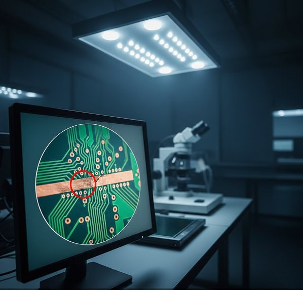
9. What are the common challenges in pcb etching quality?
The most common challenges in pcb etching involve managing the “undercut” effect and ensuring uniform copper removal across large panels. Here’s the deal: as the chemical eats downward through the copper, it also eats horizontally underneath your protective mask. If this isn’t accounted for in the original design, your traces could end up too narrow to carry the required current. This is particularly dangerous for mixed assembly boards that carry high power.
How do we overcome physical etching limitations?
We use “etch compensation” during the design phase to widen the traces on the film, anticipating the copper that will be lost in the bath. ● Undercut Management: High-pressure oscillating sprays minimize lateral erosion. ● Puddling Solutions: Fresh chemicals break up the “pool” of spent etchant on top of the board. ● Surface Prep: Precision pre-cleaning ensures no contamination acts as a secondary resist.
You might be wondering how we catch these microscopic errors before they reach the assembly line. We utilize Automated Optical Inspection (AOI) to scan every single board after it leaves the etching chamber. This level of expertise is why we are a preferred pcb assembly partner for engineers who demand perfection.
Key Takeaway
Engineering around the limitations of chemistry is what separates an average manufacturer from a world-class partner.
| Defect | Cause | Prevention |
| Over-Etching | Slow conveyor speed | Speed calibration |
| Under-Etching | Weak concentration | Auto-dosing |
| Pinholes | Dirty imaging | Cleanroom standards |
10. How can you optimize your design for better pcb etching results?
Optimizing your design for pcb etching involves following DFM (Design for Manufacturing) rules that respect the physical limits of chemistry. This is where it gets interesting… simple changes like widening traces that aren’t space-critical or avoiding 90-degree “acid traps” can drastically improve your board’s reliability. When you design for the process, you ensure that your product can be built repeatedly and at a lower cost.
What are the top DFM tips for etching?
Designers who work closely with their fabricators often see a 15-20% increase in production yield. ● Avoid Acid Traps: Keep corners at 90 degrees or larger to prevent chemical pooling. ● Consistent Copper Density: Use copper pours to balance etchant consumption across the panel. ● Generous Spacing: Keep traces further apart where space allows to give the etchant room to flow.
Ready for the good part? At QueenEMS, our engineers perform a full DFM review on your files before we ever start the etching process. We help you find the “acid traps” so your hardware startups don’t have to learn the hard way.
Key Takeaway
Design for Manufacturing isn’t just a buzzword; it’s the most effective way to lower costs and increase the reliability of your boards.
| DFM Rule | Benefit | Implementation |
| No 45-degree traps | Prevents over-etching | Routing check |
| Copper Thieving | Ensures uniform trace width | Layout addition |
| Minimum Spacing | High yield rates | Design rule check |
Conclusion
PCB Etching 101: Methods, Process Steps, and Best Practices has detailed the critical journey from a solid copper sheet to a refined, high-performance circuit. We have covered everything from the fundamental chemistry of alkaline and acidic baths to the high-tech precision of plasma and laser alternatives. The main finding is clear: etching is a surgical process that requires constant monitoring and expert design to achieve zero-defect reliability. By mastering these steps, you ensure your smt assembly rests on a perfect foundation. We recommend partnering with a manufacturer that understands the deep physics of fabrication to avoid the hidden costs of failures. QueenEMS is dedicated to being that partner, providing the technical edge your business needs to succeed. If you are ready to ensure your next project is built with world-class precision, contact us today.
FAQ
Q1: What is pcb etching? PCB etching is the chemical or physical process of removing unwanted copper from a circuit board to reveal the intended signal traces.
Q2: How does the alkaline etching process work? It works by using an ammonia-based solution that dissolves copper while being chemically indifferent to the tin resist protecting your circuit.
Q3: Can I use acidic etching for all layers? Generally, it is used for inner layers where photoresist is present, but it cannot be used on outer layers with tin resists as it would dissolve the protective plating.
Q4: Why is my board experiencing undercutting? Undercutting is a natural part of wet etching where the chemical eats horizontally; it is managed by adjusting spray pressure and etchant strength.
Q5: Is laser etching suitable for high-volume production? Currently, it is best for rapid prototyping because the beam must trace every line, making it much slower than the batch chemical processes used for large orders.