
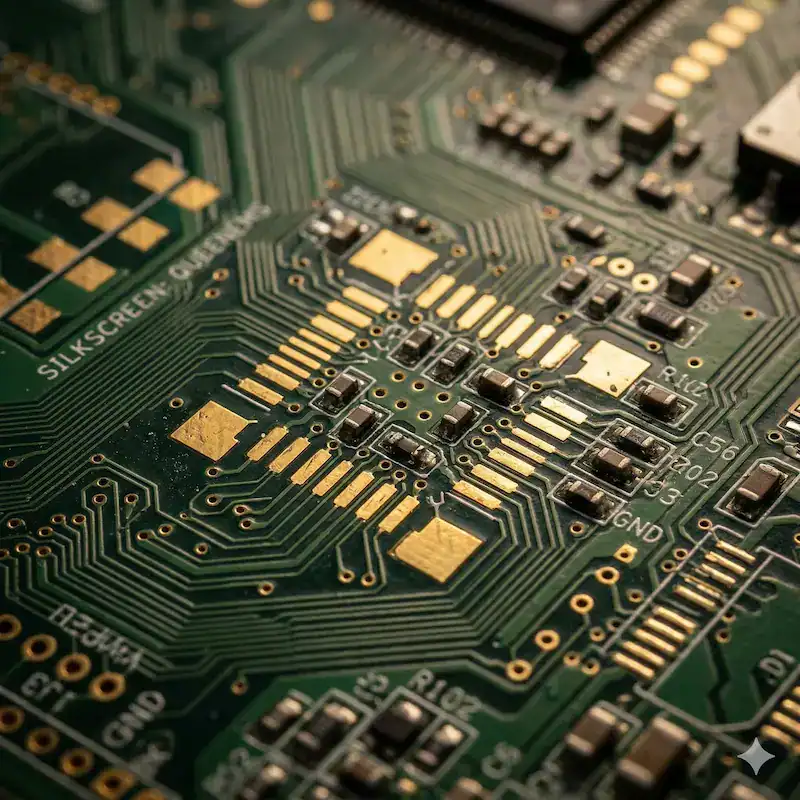
What is a multilayer pcb? A multilayer PCB represents a complex circuit board comprising three or more conductive copper layers separated by insulating dielectric materials and bonded under high pressure. You might be wondering why your current high-speed electronic projects suffer from signal lag or excessive electromagnetic interference despite using quality components. This frustrating scenario often stems from using outdated double-sided layouts that cannot handle the dense routing required by modern 5G or AI processors. Fortunately, transitioning to a professional multilayer pcb structure provides the shielding and space efficiency necessary for peak performance. At QueenEMS, our engineering team optimizes these complex stackups to ensure your B2B product launches without technical delays or manufacturing errors.
1. What exactly is a multilayer pcb in modern electronics?
A multilayer pcb functions as an advanced vertical wiring platform featuring multiple internal signal and plane layers within a single rigid or flexible substrate. Here is the deal: while standard boards limit routing to two surfaces, these sophisticated components utilize internal copper planes to achieve incredible circuit density. This stacked architecture allows engineers to integrate thousands of interconnections into a minimal physical footprint which remains vital for aerospace and high-end server hardware. Utilizing a multilayer pcb from a certified factory guarantees that your design maintains structural integrity while supporting the most demanding electrical functions.
How many layers can you realistically stack today?
Industrial applications commonly utilize between four and twelve layers, yet ultra-complex medical or telecommunications systems often require thirty-two layers to operate effectively. But here’s the kicker; increasing layer counts demands extreme precision in lamination because even minor misalignment ruins the entire production batch instantly. Every additional copper sheet provides new opportunities for dedicated ground shielding or efficient power distribution across your entire electronic assembly. Modern fabrication facilities use laser-guided registration tools to ensure that these dense stacks remain perfectly aligned throughout the long manufacturing journey.
How do internal layers communicate with the surface?
Vertical communication between conductive levels relies on plated-through holes called vias which can be through-hole, blind, or buried depending on layout needs. You might be wondering if these tiny internal connections survive the intense heat cycles of repeated SMT reflow or harsh field operation. Because layers bond under vacuum using high-flow resin, the finished structure becomes a robust monolithic block resistant to thermal expansion or mechanical warping. This seamless connectivity allows high-speed microprocessors to exchange data with peripheral chips with virtually zero signal loss or latency issues.
| Layer Category | Target Industry | Complexity Level | Typical Thickness |
|---|---|---|---|
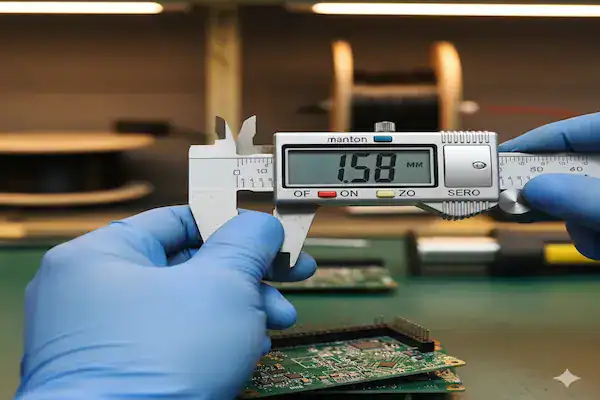
| 4-6 Layers | Consumer IoT | Standard | 1.0mm – 1.6mm |
| 8-14 Layers | Industrial Automation | High | 1.6mm – 2.0mm |
| 16-32 Layers | Server / Aerospace | Ultra-High | 2.4mm+ |
The data above illustrates how layer count directly determines the technical capability and suitable application environment for your project.
Key Takeaway: Understanding the vertical structure of these boards helps you realize why they represent the gold standard for high-density electronic packaging.
2. How is a multilayer pcb constructed during fabrication?
The construction of a multilayer pcb involves a highly controlled sequence where alternating sheets of copper-clad core and prepreg resin bond together. Believe it or not, the quality of this internal bond determines the entire operating life of your device, especially in high-vibration automotive environments. Each inner layer receives independent etching of circuit patterns before stacking occurs within a cleanroom to prevent microscopic dust from causing shorts. This meticulous buildup creates a solid composite foundation that provides both reliable electrical paths and the mechanical rigidity required for assembly.
What role does the prepreg play in the stack?
Prepreg serves as the essential “glue” that melts and cures to hold various copper layers together while providing critical electrical insulation. This is where it gets interesting because resin content and glass weave style directly influence the final thickness and dielectric constant of your circuit board. Selecting the correct prepreg helps maintain stable impedance across high-frequency traces which prevents data corruption in sensitive telecommunications equipment. Our experts often provide a free technical review to ensure your material stackup aligns perfectly with manufacturing tolerances and project goals.
Why is inner layer registration so difficult to master?
Maintaining perfect alignment across ten or twenty hidden layers requires advanced optical registration systems that detect deviations smaller than a human hair. The catch is that if one layer shifts during the high-pressure pressing cycle, drilled vias will miss their pads and fail electrically. High-end factories utilize real-time X-ray inspection tools to verify internal registration after lamination but before any outer layer processing starts. This critical step guarantees that every internal connection remains solid so that your high-value components function exactly as designed.
| Material Block | Main Function | Thermal Limit | Relative Price |
|---|---|---|---|
| Copper Foil | Signal Conduction | 300°C+ | Medium |
| FR4 Core | Rigid Support | 130-170°C | Low |
| Prepreg | Insulating Bond | 150°C+ | Medium |
| Specialized Substrate | High-Freq Performance | 280°C+ | High |
This material breakdown highlights the fundamental building blocks needed to construct a durable and high-performing multilayer circuit platform.
Key Takeaway: Mastering construction details allows you to design boards that are not only functional but also optimized for high-yield mass production.
Ready to Experience Zero-Risk Prototyping?
Claim your FREE 2-4 Layer FR4 Prototypes today! Partner with QueenEMS for high-precision manufacturing and turnkey assembly services — from your first design to mass production.
3. Why should you select a multilayer pcb for your project?
Selecting a multilayer pcb provides overwhelming benefits in size reduction and electrical performance that simpler double-sided boards cannot possibly match. Ready for the good part? By stacking circuitry vertically, you can drastically reduce the physical volume of your product, allowing for the sleek designs that B2B clients expect. This increased density enables engineers to pack more processing power and features into a single module, which remains essential for drones and medical devices. A well-designed multilayer pcb acts as the central nervous system for your hardware, ensuring all signals travel reliably and quickly.
Can these boards improve your signal integrity?
Absolutely, because adding dedicated ground and power planes creates a stable electromagnetic environment that shields sensitive data traces from external noise. What’s the real story? Internal layers allow for stripline configurations that control impedance with much greater precision than surface routing alone can ever achieve. This leads to cleaner signals, significantly reduced cross-talk, and faster transmission speeds which are vital for high-performance computing systems. By isolating high-speed paths within internal layers, you effectively armor your data against the electrical chaos of modern crowded circuit environments.
How do they manage heat better than standard boards?
While dense layouts might seem prone to overheating, large internal copper planes actually function as effective heat sinks that spread thermal energy. Wait, there’s more; by strategically placing thermal vias, you can move heat away from power-intensive processors much more effectively than on single-layer boards. This thermal management capability extends the lifespan of your components and prevents catastrophic failures caused by localized hotspots during peak processing loads. Effective heat dissipation represents a primary reason why top engineers choose these boards for automotive motor controllers and power electronics.
| Advantage Type | Impact on Design | Long-Term Value | Priority Level |
|---|---|---|---|
| Space Saving | 60% – 80% Reduction | High | Essential |
| EMI Control | Superior Noise Shielding | Medium | Critical |
| Signal Speed | Optimized Data Paths | High | High |
| Weight Reduction | Lightweight Polyimide Options | High | Important |
These benefits clearly demonstrate why multi-layered boards remain the preferred platform for sophisticated, market-leading electronic innovations globally.
Key Takeaway: Choosing a multilayer design represents a strategic investment in both product miniaturization and the long-term reliability required by industrial users.
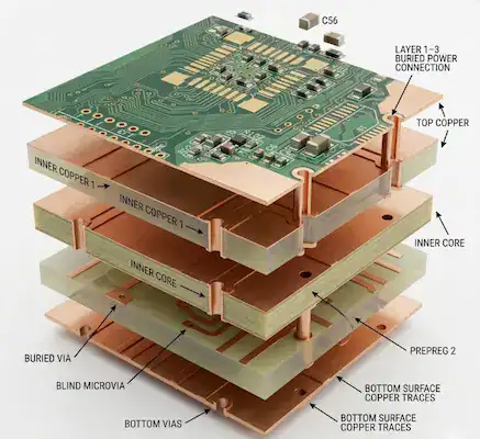
4. What are the core components of a multilayer pcb stackup?
A multilayer pcb stackup serves as primary skeletal framework within your electronic design projects today. Balanced arrangements remain vital because they prevent board bowing during long fabrication cycles in factories. It gets better; properly configured heavy copper layers enhance thermal dissipation while guaranteeing consistent electrical characteristics. Our factory team evaluates every layer arrangement carefully to maximize magnetic flux cancellation effect. This specific engineering step significantly reduces electromagnetic footprint across your industrial device modules. Choosing symmetrical patterns protects structural integrity while supporting high-speed processing requirements effortlessly. Every additional plane provides fresh opportunities regarding dedicated ground shielding or efficient power distribution systems. Proper planning avoids signal reflections that ruin data integrity within sophisticated telecommunication equipment components. Understanding vertical structure remains fundamental step toward achieving high-yield mass production outcomes. B2B buyers prioritize reliability which begins with professional stackup planning from expert manufacturing partners.
How do you optimize 4-layer and 6-layer stackups for reliability?
For four-layer boards, standard Top-GND-VCC-Bottom stackups prevail across most B2B manufacturing industries. True optimization requires keeping signal layers extremely close against adjacent ground reference planes. But here’s the kicker; moving into six-layer designs allows implementing stripline configurations for superior noise shielding. High-speed traces sit sandwiched between two solid internal copper planes within these high-reliability boards. This specific arrangement remains ideal choice regarding industrial robotics or mission-critical IoT gateways. Utilizing 1.6mm thickness maintains mechanical rigidity while providing enough space for high-quality prepreg materials. Consistent copper weights guarantee even thermal expansion during automated smt assembly operations. Designers should prioritize Layer 2 as solid ground plane for reliable signal return paths. Shortening distance between Layer 1 and Layer 2 improves electromagnetic compatibility results dramatically. Advanced stackups include high-resin prepregs that fill gaps within dense circuit patterns effectively.
What is the secret to 8-layer board signal integrity?
Eight-layer boards represent pinnacle regarding high-speed digital design for advanced 5G hardware. Achieving perfect signal integrity demands absolute mechanical symmetry around center core substrate material. Ready for the good part? Matching copper distribution between layer pairs like L1/L8 prevents problematic warping. This stability protects fine-pitch BGA solder joints during intense production soldering cycles. Experienced engineers place ground planes directly adjacent every signal layer for shortest return paths. Low loop inductance results from continuous internal planes free from large splits or gaps. Symmetry remains non-negotiable step securing production yields exceed ninety-eight percent quality threshold. Utilizing multiple reference planes supports extreme data rates found inside modern AI processing units. Careful material selection prevents delamination under harsh thermal conditions found in automotive sectors. Maintaining tight impedance control involves precise thickness management across every dielectric sheet used.
How can you reduce manufacturing costs through stackup optimization?
Reducing multilayer pcb costs involves simplifying manufacturing processes rather than using cheaper raw materials. You often save thirty percent by sticking with standard through-hole via designs. Adding two extra layers usually costs less compared against expensive blind via drilling technology. What’s the real story? Specifying standard impedance tolerance like plus-minus ten percent allows much higher factory yields. QueenEMS provides 2-hour fast quotes featuring free DFM review technical sessions. We help identify hidden savings before you finalize complex purchase orders. Optimization includes efficient panelization which fits more boards onto single 18×24 production sheets. Avoid blind vias unless space constraints remain absolute for medical implants or wearables. Proper design for manufacturing principles guarantee your project stays within budget boundaries. Factories operate efficiently when Gerber files follow standard fabrication limits regarding trace widths.
| Layer Count | Shielding Level | Design Complexity | Cost Optimization Potential |
|---|---|---|---|
| 4 Layers | Basic | Low | High (via panelization) |
| 6 Layers | Excellent | Medium | Medium (via trace routing) |
| 8 Layers | Ultra-High | High | Strategic (via through-hole use) |
This technical breakdown illustrates how layer selection and stackup planning directly influence both electrical success and final cost.
Ready to Experience Zero-Risk Prototyping?
Claim your FREE 2-4 Layer FR4 Prototypes today! Partner with QueenEMS for high-precision manufacturing and turnkey assembly services — from your first design to mass production.
Key Takeaway: Symmetrical stackup planning and avoiding high-complexity via types remain most effective ways balancing performance with manufacturing budgets.
5. How do vias function within a high-density multilayer pcb?
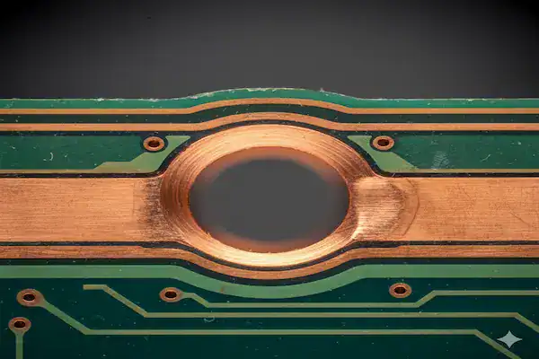
Vias serve as the vertical conduits that allow electrical signals to travel between different levels of a multilayer pcb without using surface space. But here’s the kicker; in high-density designs, standard through-hole vias often occupy too much area, requiring the use of blind or buried technologies. These specialized holes connect only the specific layers required, leaving other layers free for routing or plane coverage to maximize density. Integrating advanced microvias into a multilayer pcb design remains the secret to achieving the extreme miniaturization seen in medical implants.
What is the difference between blind and buried vias?
Blind vias connect an outer layer to internal layers but do not pass through the entire board, making them hidden from one side. You might be wondering how buried vias differ; these are entirely contained within internal layers and have no connection to either external board surface. This capability allows you to stack connections vertically through the board, freeing up massive amounts of routing space for dense BGA components. Utilizing these techniques increases manufacturing complexity but provides unparalleled design freedom for the most challenging electronic packaging projects in your pipeline.
How does via-in-pad technology help your layout?
Via-in-pad technology involves placing a microvia directly inside a component’s solder pad and plating it shut with copper to create flatness. Here is the deal: this technique eliminates the need for traditional dog-bone fanouts, which saves precious space and reduces parasitic inductance issues. This remains particularly useful for fine-pitch BGA chips where every micron of space is vital for routing out hundreds of sensitive pins. While it adds cost due to extra plating steps, the performance and space gains often justify the investment for cutting-edge hardware.
| Via Technology | Starting Layer | Ending Layer | Manufacturing Difficulty |
|---|---|---|---|
| Through-Hole | Top Surface | Bottom Surface | Standard |
| Blind Via | Outer Layer | Inner Layer | Advanced |
| Buried Via | Inner Layer | Inner Layer | Advanced |
| Laser Microvia | Layer N | Layer N+1 | Ultra-High (HDI) |
Each via type offers a unique balance between routing density and fabrication cost, allowing you to tailor your design to specific project needs.
Key Takeaway: Strategically using various via technologies allows you to maximize routing density while maintaining a stable and manufacturable circuit board design.
6. Which materials are best for high-performance multilayer pcb?
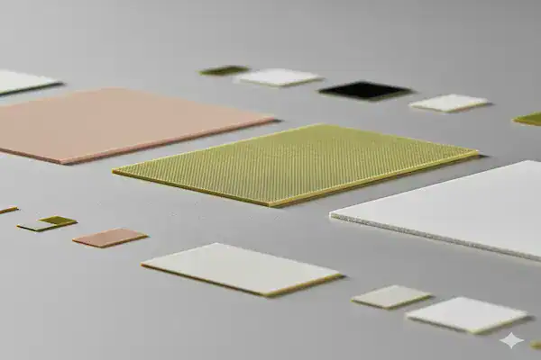
Choosing the right materials for a multilayer pcb depends heavily on your operating frequency, thermal environment, and the final application needs. Believe it or not, standard FR4 is adequate for most consumer products, but 5G applications require advanced substrates like Rogers to minimize signal loss. These specialized materials offer much lower dielectric loss tangents and stable dielectric constants across a wide range of temperatures and frequencies. Investing in high-quality materials for your multilayer pcb ensures that your product performs reliably in the field under demanding conditions.
Why is Tg (Glass Transition Temperature) important for reliability?
The Tg value indicates the temperature where base material starts to soften and expand rapidly, which can lead to internal via cracking. The catch is that for multilayer designs, you should specify High-Tg FR4 to withstand the multiple heat cycles required for assembly. This increased thermal stability protects your internal connections and guarantees that the board remains flat throughout its entire operating service life. Always consult with your manufacturing partner to ensure the material you select can handle your specific assembly and environmental temperature requirements.
Are there materials for extreme thermal environments?
For applications like engine controls, ceramic-based PCBs or metal core boards offer superior thermal conductivity compared to standard organic FR4 substrates. Wait, there’s more; polyimide materials used in flexible circuits can also handle extreme temperatures without losing their mechanical or electrical properties. These materials allow you to place electronics in environments that would melt standard boards, expanding possibilities for aerospace and automotive engineering. Choosing the right material grade early in the design process represents the most effective way to prevent costly field failures.
| Material Grade | Dielectric Loss (Df) | Max Temp (Tg) | Main Application |
|---|---|---|---|
| Standard FR4 | 0.020 | 130°C | Consumer Goods |
| High-Tg FR4 | 0.015 | 170°C+ | Industrial / Automotive |
| Rogers 4350B | 0.0037 | 280°C | 5G / RF Signal |
| Polyimide (Flex) | 0.010 | 250°C+ | Foldable Electronics |
This comparison chart helps you identify the best material choice based on the technical performance needs of your specific circuit design.
Key Takeaway: Matching material properties to your application environment is essential for achieving the best balance between performance, reliability, and manufacturing cost.
7. What are the essential design rules for multilayer pcb?
Implementing correct design rules for a multilayer pcb remains vital for ensuring that your board can be manufactured with high yields. You might be wondering why your current designs get flagged during DFM checks; it is often due to traces being too close. These rules provide necessary buffers that account for natural variations in the fabrication process, such as layer shifting or drill wander. Adhering to strict design standards for your multilayer pcb significantly reduces the risk of expensive redesigns and mass production delays.
How do you manage trace width and spacing?
Maintaining consistent trace width and spacing is essential for impedance control and for preventing electrical shorts between densely packed signal lines. The truth is that as you increase layers, traces become thinner to accommodate more connections, which requires high-end fabrication equipment. You must also consider the copper weight; thicker copper requires wider spacing to allow etching chemicals to remove metal cleanly between traces. Designing with these manufacturing limits in mind ensures that your boards are reliable and that signal paths remain clean and conductive.
Why should you keep traces away from the board edge?
Placing traces or planes too close to the board edge can lead to copper exposure or delamination during final routing. This is where it gets interesting because exposed copper causes short circuits when the board mounts in a metal enclosure or during assembly. A standard rule involves keeping all conductive elements at least 0.5mm away from the edge to provide a safe mechanical buffer. This simple precaution protects your internal circuitry from moisture and physical damage, enhancing the long-term durability of your final electronic assembly.
| Design Rule | Standard Spec | Premium Spec | HDI Spec |
|---|---|---|---|
| Min Trace Width | 0.125mm (5mil) | 0.075mm (3mil) | 0.050mm (2mil) |
| Min Trace Spacing | 0.125mm (5mil) | 0.075mm (3mil) | 0.050mm (2mil) |
| Annular Ring | 0.150mm (6mil) | 0.100mm (4mil) | 0.050mm (2mil) |
| Edge Clearance | 0.500mm (20mil) | 0.300mm (12mil) | 0.200mm (8mil) |
Following these guidelines ensures your layout is optimized for both manufacturing reliability and electrical performance across all internal copper layers.
Key Takeaway: Adopting conservative design rules during the layout phase remains the most effective way to guarantee high production yields and integrity.
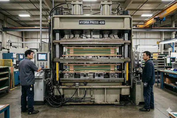
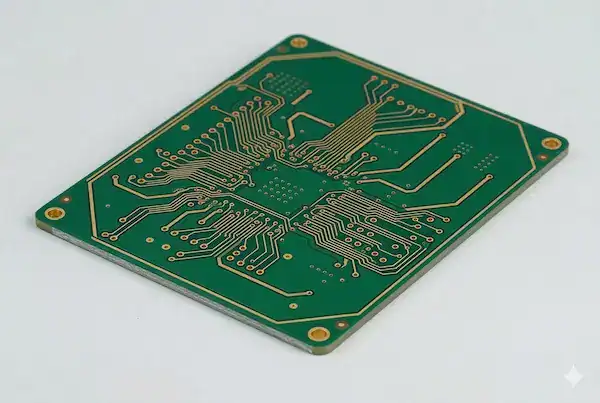
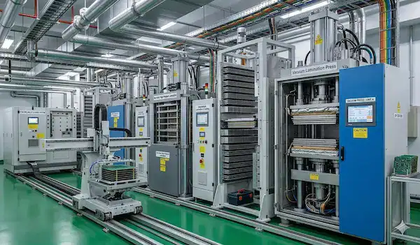
8. How does the manufacturing process for multilayer pcb work?
The manufacturing process for a multilayer pcb represents a complex journey beginning with inner layer imaging and ending with final inspection. Ready for the good part? Each internal layer is etched independently before being stacked and bonded in a massive hydraulic press under precise temperature profiles. This ensures that resin flows correctly to fill all gaps between traces, creating a perfectly solid and insulated composite circuit board. Working with a professional factory for your multilayer pcb needs ensures that every step is monitored by advanced AOI systems.
What happens during the critical lamination phase?
During lamination, stacked layers are subjected to intense heat and pressure which causes prepreg resin to melt and then cure. But here’s the kicker; if the temperature ramp-up is too fast, internal air bubbles or voids form, leading to board failure. Precise control over this cycle separates high-quality manufacturers from low-cost providers who might cut corners on press time to save money. A perfectly laminated board provides the stable foundation needed for accurate drilling and high-quality through-hole plating in subsequent manufacturing steps.
How are high-density vias drilled with such accuracy?
In multilayer designs, drilling uses high-speed CNC machines or precision UV lasers for the tiny microvias required by HDI technology. You might be wondering how the drill knows where to go if internal pads are hidden; factories use X-ray systems. This compensates for any minor layer shifting that occurred during lamination, ensuring that every via makes a solid electrical connection. This level of technical sophistication is necessary to produce the dense, reliable boards required for modern aerospace and medical electronics.
| Process Step | Primary Objective | Machine Used | Accuracy Check |
|---|---|---|---|
| Inner Etching | Form Circuit Patterns | Chemical Etcher | AOI Scan |
| Lamination | Bond Layers Together | Vacuum Press | X-Ray Registration |
| CNC Drilling | Create Through-Holes | High-Speed Drill | Visual Inspection |
| Plating | Connect Layers | Electroplating Tank | Cross-Sectioning |
This workflow illustrates the critical milestones required to transform raw materials into a high-precision, multi-layered circuit board for industrial use.
Key Takeaway: Understanding the manufacturing journey allows you to appreciate the extreme precision required to deliver a reliable, high-performance multilayer circuit.
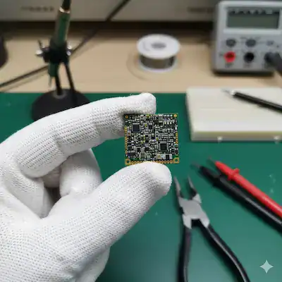
9. Where do we typically see multilayer pcb applications today?
Today, multilayer pcb applications dominate every sector of the electronics market, from smartphones to advanced medical imaging systems in hospitals. Wait, there’s more; as technology shrinks and data speeds increase, the demand for high-layer-count boards expands into robotics and drones. These boards represent the only solution that can handle the massive data and power distribution required by modern AI processors. A high-quality multilayer pcb remains the fundamental building block for any product aiming for market leadership in B2B.
Why are they essential for 5G telecommunications?
5G technology operates at extremely high frequencies where even slight signal interference leads to massive data loss and dropped connections. What’s the real story? Multilayer boards allow the creation of complex shielding structures and precisely controlled impedance traces that keep high-frequency signals clean. By isolating noisy power traces from sensitive RF signals within internal layers, engineers achieve the ultra-fast speeds that users expect. This level of performance is impossible to achieve with older, single or double-sided board designs using standard materials.
How do they support the growth of Internet of Things?
The Internet of Things (IoT) requires billions of tiny connected sensors that must be small enough to integrate into everyday objects. Here is the deal: multilayer designs allow these devices to include a processor, wireless antenna, and power management on one tiny board. This extreme miniaturization drives innovation in wearable health trackers, smart home devices, and industrial monitoring systems that save company money. As the IoT market explodes, the reliance on dense, multi-layered circuit boards will continue to grow, making them vital parts.
| Industry Sector | Primary Requirement | Layer Count Range | Core Material |
|---|---|---|---|
| Medical Devices | Reliability / Size | 4 – 10 Layers | High-Tg FR4 |
| Telecom (5G) | Signal Integrity | 12 – 24 Layers | Low-loss Rogers |
| Automotive | Vibration Resistance | 4 – 8 Layers | Heavy Copper |
| Consumer IoT | Cost / Miniaturization | 4 – 6 Layers | Standard FR4 |
This table shows how different industries tailor their multilayer board specifications to meet their unique technical and market challenges effectively.
Key Takeaway: From deep-sea sensors to orbiting satellites, multilayer boards serve as the essential platform for the next generation of high-tech innovation.
10. How to choose the right multilayer pcb manufacturer now?
Choosing the right multilayer pcb manufacturer represents a critical business decision that determines the success of your entire product launch. Believe it or not, many manufacturers claim to handle complex boards but lack the specialized X-ray inspection equipment needed for reliability. You need a partner who offers transparent communication, fast 2-hour quotations, and comprehensive engineering support to catch potential design flaws. Partnering with a proven factory like QueenEMS guarantees that your multilayer pcb orders receive the highest professional care.
Should you look for specific international certifications?
Yes, you should always verify that your manufacturer holds authentic ISO 9001, UL, and RoHS certifications to ensure quality standards. The catch is that these certifications represent your only guarantee that the factory uses high-quality raw materials and follows audits. At QueenEMS, we pride ourselves on maintaining total transparency with clients, providing full documentation and material traceability for every production batch. This commitment to quality protects your brand reputation and ensures that your final products remain safe and compliant for markets.
What role does engineering support play in your success?
A manufacturer providing direct access to seasoned PCB engineers helps you optimize your stackup for both cost and performance goals. This is where it gets interesting because a good engineering team suggests material alternatives or via modifications that improve your yield. We offer a 100% free DFM review for every project to ensure your files are optimized for our automated production lines. This proactive approach eliminates delivery delays and guarantees that you receive perfect boards on the very first shipment without rework.
| Selection Metric | Importance | Business Impact | QueenEMS Feature |
|---|---|---|---|
| Advanced Machines | Critical | High Reliability | 100+ Automated Units |
| Engineering DFM | High | Cost Savings | Direct Engineer Access |
| Certification | Essential | Market Compliance | ISO/UL/RoHS Certified |
| Quote Speed | Medium | Faster Timelines | 2-Hour Response Time |
Evaluating these factors carefully will lead you to a manufacturing partner who can grow with your business and handle challenges.
Key Takeaway: Selecting a manufacturer with deep technical expertise and modern equipment remains the most effective way to secure your supply chain.
Conclusion
In summary, multilayer PCB design represents the pinnacle of modern electronic packaging, offering the density, speed, and reliability required for today’s B2B applications. We have covered everything from fundamental construction and material choices to advanced via technologies and essential design rules needed for success. This is where it gets interesting; while the technical challenges are significant, partnering with the right experts allows you to turn these challenges into a powerful competitive advantage. At QueenEMS, our vision involves empowering global innovators by providing world-class manufacturing services that bridge the gap between complex design and production. Whether you are scaling a new robotics project or launching a 5G module, we are committed to delivering the precision you need. Please contact us today to discuss your next multilayer project and experience the difference that factory-direct engineering support makes.
FAQ Section
Q1: How do I know if my high-speed signals require Rogers material instead of High-Tg FR4? It depends primarily on your operating frequency; generally, if your signals exceed 5GHz or require ultra-low signal loss for RF applications, Rogers is the best choice. While High-Tg FR4 is cost-effective for most high-speed digital applications, Rogers provides the stable dielectric constant and low dissipation factor needed for peak microwave performance.
Q2: What’s the best way to configure an 8-layer stackup to minimize EMI? The most effective strategy involves placing solid ground planes directly adjacent to every high-speed signal layer throughout the stack. This creates a tight return path and minimizes loop inductance, which remains the primary cause of electromagnetic interference in complex industrial and telecommunication designs.
Q3: Can I use via-in-pad technology on a 4-layer board to save space? Yes, you certainly can; although via-in-pad is more common in high-density HDI designs, it is an excellent way to route out fine-pitch components on standard 4-layer boards. It frees up precious surface space for additional components while significantly improving the thermal and electrical performance of the connection for better reliability.
Q4: How do I know if my trace width and spacing meet your factory’s manufacturing limits? The best way is to submit your Gerber files for our 100% free DFM review before you place your order. While our standard manufacturing limit is 3-4 mils for high-density boards, our engineering team will check your specific layout to ensure it aligns perfectly with our automated etching and plating capabilities to prevent any production shorts.
Q5: Can I get a consolidated quote that includes both PCB fabrication and full BOM sourcing? Yes, we offer comprehensive turnkey services that cover everything from raw board manufacturing to component procurement and final assembly. This “one-stop” approach significantly reduces your administrative overhead and eliminates the logistical risks associated with coordinating multiple vendors for a single project.
Q6: How do I know if choosing a higher layer count will actually lower my total project cost? Sometimes increasing layer counts—for example, moving from a 4-layer to a 6-layer design—allows you to drastically shrink the overall board size and utilize a cheaper, smaller enclosure. Our engineers can perform a detailed cost-benefit analysis to see if increased vertical density leads to overall savings in your product’s total bill of materials.
Q7: What’s the best way to optimize panel utilization to reduce the price per unit? The best method is to consult our engineering team during your layout phase; minor adjustments to your board dimensions, even as small as 2-3mm, can often allow more boards to fit on a standard production panel. This instantly lowers your per-unit cost without sacrificing any functionality or performance for your final product launch.
Q8: How do I know if there are hidden NRE or tooling costs in my multilayer pcb quotation? At QueenEMS, we provide transparent, itemized quotes with absolutely no hidden fees for our B2B partners. Any one-time engineering (NRE) or stencil costs are clearly listed upfront in the initial quote, ensuring you can accurately budget for both your initial prototypes and your subsequent mass production runs.
Q9: What’s the best way to transition my project from a 7-day prototype to a high-volume production run? The most reliable path is to utilize the same manufacturing partner for both the prototyping and mass production stages. Because we use identical process parameters and equipment for both, you won’t face the “re-tooling” surprises or quality shifts that often occur when moving between different factories with different capabilities.
Q10: How do I know if my multilayer pcb project will pass international certifications like UL or RoHS? You can trust our audited manufacturing processes; we hold valid ISO 9001 and UL certifications, and we use 100% RoHS-compliant materials for all production batches. We provide full compliance documentation with every shipment to ensure your product meets all global regulatory requirements for safety and environmental impact without delay.
Q11: Can you provide an urgent 24-hour turnaround for a complex 6-layer prototype? Yes, we maintain a dedicated “Quick-Turn” production line specifically for urgent R&D needs and critical project deadlines. Depending on the complexity and material availability, we can expedite 4-8 layer boards to be manufactured and shipped within 24-48 hours to keep your development schedule on track.
Q12: How do I know if QueenEMS can scale manufacturing as my hardware startup grows? We are specifically designed for scalability, supporting everything from 5-piece functional prototypes to 10,000+ unit mass production runs. Our facility features over 100 automated machines, ensuring that as your market demand increases, our capacity grows with you without compromising on quality or lead times.
Q13: What’s the best way to leverage your engineering expertise to improve my product’s market competitiveness? The best way is to involve our engineers early in your design process via our free DFM review service. By catching potential manufacturing defects before production starts, we help you reduce time-to-market and avoid the massive costs associated with field failures or expensive product recalls later in the lifecycle.
Q14: Can you help protect my intellectual property during the manufacturing process in China? Yes, we treat intellectual property protection as a top priority and are always happy to sign strict Non-Disclosure Agreements (NDAs). We have long-standing relationships with global B2B clients who trust our secure internal data handling and professional manufacturing ethics for their most sensitive designs.
Q15: How do I know if your quality control systems are enough to prevent expensive field failures? We utilize advanced 3D AOI and X-ray inspection on 100% of our multilayer boards to detect hidden defects like BGA shorts or internal layer misalignment. Our “zero-defect” philosophy ensures that every board leaving our factory is built to IPC Class 2 or 3 standards for maximum long-term reliability.
Q16: How do I know if my multilayer design requires a balanced stackup to prevent warping? You should always aim for mechanical symmetry around the center core to prevent bowing during the high-heat lamination process. If one side of the board has significantly more copper than the other, the resulting internal stress will cause the board to warp during soldering, making automated SMT assembly extremely difficult.
Q17: Can I choose between ENIG and OSP surface finishes for my 6-layer industrial board? Yes, you can; ENIG (Electroless Nickel Immersion Gold) is the best choice for fine-pitch BGA components due to its perfectly flat surface. While OSP is more cost-effective, it has a shorter shelf life and is less durable for multiple reflow cycles compared to the robust gold finish of ENIG.
Q18: What’s the best way to handle controlled impedance for high-speed differential pairs? The most reliable method is to provide us with your target impedance—such as 90 ohms for USB—and your proposed layer stackup. Our engineers will then adjust the trace width and dielectric spacing based on our specific material stocks to achieve the precise electrical result required for your high-speed data.
Q19: How do I know if my power distribution network requires heavy copper layers? If your traces are carrying high continuous currents or your processors are generating excessive thermal energy, heavy copper (2oz or more) is the best solution. It reduces resistive losses and acts as a massive internal heat sink, spreading thermal energy across the board to protect your sensitive components from hotspots.
Q20: Can I get a detailed DFM report before I commit to a large production order? Absolutely; we provide a comprehensive Design for Manufacturing (DFM) review as an integral part of our professional quoting process. This catches critical errors like acid traps, narrow annular rings, or insufficient solder mask clearances before you commit your budget, ensuring a smooth and successful manufacturing run.
Q21: How do I know if my design should utilize blind or buried via technology? If your routing density is so high that you cannot fit standard through-hole vias without blocking signals on other layers, blind or buried vias are the best alternative. However, be aware that they increase manufacturing complexity and cost due to the multiple lamination and drilling cycles required during the fabrication process.
Q22: What’s the best way to ensure my board passes strict Signal Integrity (SI) testing? Beyond professional routing practices, selecting low-loss substrates like Rogers or high-performance Mid-Loss FR4 is critical for success. These specialized materials maintain a stable dielectric constant across high frequencies, effectively preventing signal attenuation and timing jitter in your critical communication modules and high-speed interfaces.
Q23: Can I request IPC Class 3 manufacturing standards for my aerospace or medical project? Yes, we can manufacture to IPC Class 3 standards, which require much stricter annular ring tolerances and higher copper plating thickness in the holes. This ensures maximum electrical and mechanical reliability for mission-critical applications where field failure is simply not an option for your brand or your customers.
Q24: How do I know if my stackup is optimized for the most competitive manufacturing price? The best way is to minimize the use of non-standard dielectric thicknesses and keep copper weights consistent across all internal signal layers. Our engineers can suggest standard material alternatives that offer identical electrical performance at a lower price point, helping you maintain healthy margins for your B2B product.
Q25: What’s the best surface finish for gold wire bonding on complex multilayer PCBs? ENEPIG (Electroless Nickel Electroless Palladium Immersion Gold) is considered the “universal” finish and is the best choice for wire bonding. It provides a robust and reliable surface for both standard soldering and specialized wire bonding, making it ideal for high-reliability medical or military electronic modules.
Q26: How do you handle ‘copper thieving’ on internal planes to ensure even plating? We automatically add non-functional copper patterns to sparse areas of your signal layers during our advanced CAM processing stage. This ensures uniform plating thickness across the entire board surface and prevents the mechanical warping caused by unbalanced copper distribution during the high-pressure lamination cycle.
Q27: Can I request a cross-section report to verify the quality of internal layer registration? Yes, we can provide microscopic cross-section images and reports upon request for your quality documentation. This allows you to verify the copper plating thickness within the vias and the perfect alignment of internal pads with the drilled holes, providing total peace of mind for your engineering team.
Q28: How do I know if my design has ‘acid traps’ that could cause trace thinning? Acid traps are sharp-angled traces—usually less than 90 degrees—that trap etching chemicals, leading to potential trace thinning or open circuits. Our DFM review automatically flags these issues, allowing our engineers to smooth out the angles and ensure a reliable, long-lasting circuit for your industrial application.
Q29: What’s the best way to manage multiple power rails in a dense 10-layer board? The most effective strategy is to utilize split power planes on dedicated internal layers. By carefully isolating different voltage zones within a single copper plane, you can provide clean power to all your chips without adding excessive layers or thickness, keeping your design both compact and cost-effective.
Q30: How do I know if QueenEMS is the right long-term partner for my scaling hardware business? We focus on being the “bridge” from your initial R&D prototypes to full-scale mass production. By offering the same level of technical support and quality standards for a 5-piece order as we do for a 10,000-piece run, we ensure a smooth, risk-free growth path for your brand in the global market.