
Quick Answer: A transistor pinout defines the specific physical arrangement of terminals (Emitter/Base/Collector for BJTs, or Gate/Drain/Source for MOSFETs) required for correct circuit integration. Over 60% of component orientation defects in PCB assembly stem from mismatching generic datasheets with specific package types like TO-92 or SOT-23. Key takeaways:
- TO-92 packages have no universal standard; a 2N2222 can be E-B-C or C-B-E depending on the manufacturer.
- Verifying BJT junctions requires a multimeter with millivolt precision, as E-B drops are only 20–50mV higher than C-B drops.
- MOSFETs demand stricter ESD control during handling because their gate oxide layers are merely 2-10nm thick.
- Cross-referencing exact Manufacturer Part Numbers (MPNs) against PCB footprints prevents costly assembly reworks.
Table of Contents
- 1. What Is a Transistor Pinout and Why Does It Matter for PCBA?
- 2. How Do You Identify BJT Pin Configurations Correctly?
- 3. How Do Different Packages Affect Component Layouts?
- 4. What Are the Exact Pin Sequences for 30+ Transistors?
- 5. What Are the Key Differences in MOSFET Transistor Pinouts?
- 6. How Can You Verify Unknown Parts with a Multimeter?
- 7. Why Does the Same Part Number Have Different Lead Orders?
- 8. How to Prevent Transistor Pinout Errors in BOM and PCB Design?
- 9. How Do Assembly Factories Catch Orientation Defects?
- 10. Can You Swap Devices If the Transistor Pinout Matches?
A transistor pinout dictates the exact physical connections needed to route electrical signals through a semiconductor component. You stare at a freshly assembled PCB, only to realize the entire batch fails power-up testing because the generic library footprint did not match the physical component. This mismatch forces expensive rework, delays shipping schedules, and ruins perfectly good boards. You can stop these alignment failures by referencing exact transistor pinout data mapped directly to manufacturer specifications before you ever finalize your BOM. To keep this data handy at your workbench, we highly recommend you download the complete Transistor Pinout PDF Cheat Sheet (Free) for offline reference.
1. What Is a Transistor Pinout and Why Does It Matter for PCBA?
A transistor pinout determines the specific functional assignment of each physical metal lead extending from a semiconductor package. Incorrect pinouts cause immediate short circuits or open lines, which means the SMT assembly process will mount parts that inherently cannot function. A footprint is the physical copper land pattern on a PCB. It must align perfectly with component leads, resulting in an assembly with a 99.7% first-pass yield.
Defining Component Layout Specifications
Pinout mapping assigns logic to physical space. If you swap the emitter and collector on a BJT, the circuit enters reverse active mode with a current gain (beta) dropping below 1. Consider this reality:
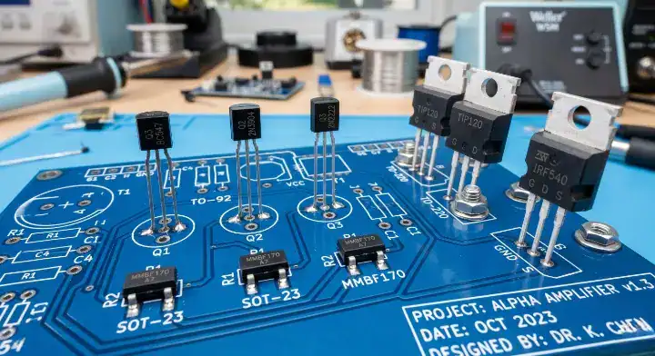
- Standard SOT-23 packages have three physical pins.
- Pin 1 is typically assigned to the Base or Gate.
- Misalignment causes instant thermal runaway.
The Manufacturing Impact of Misalignment
Incorrect pad assignments force factories to manually desolder and rotate components, adding $1.50 per rework cycle. You lose time and money when the footprint does not match the actual silicon.
| Defect Type | Immediate Consequence | Rework Cost |
|---|---|---|
| 180-Degree Rotation | Dead circuit, blown fuse | High |
| Emitter/Collector Swap | Low gain, signal distortion | Medium |
| Gate/Source Swap | Absolute failure to switch | High |
Analysis: Misaligned pins destroy functional yield because automated optical systems cannot catch electrical polarity errors inside symmetrical packages.
Key Takeaway: The physical sequence of leads must match the schematic symbol perfectly. Bottom line: Always cross-reference the manufacturer’s exact datasheet against your CAD library before releasing Gerber files.
2. How Do You Identify BJT Pin Configurations Correctly?
Identifying a BJT transistor pinout requires mapping the physical legs to the Emitter, Base, and Collector functions. NPN and PNP variants often share identical physical packages, which means you cannot rely on visual inspection alone to determine the internal polarity. You must read the specific datasheet diagram and note the designated view direction.
Differentiating NPN and PNP Structures
Bipolar Junction Transistors operate by injecting current into the middle layer. NPN types require positive voltage at the Base, while PNP types need negative voltage relative to the Emitter. Here is the truth:
- NPN transistors source current from the Collector to the Emitter.
- PNP transistors source current from the Emitter to the Collector.
- The Base pin acts as the main current control valve.
The View Direction Trap
Engineers frequently misread datasheets because “bottom view” and “top view” diagrams look completely different. Looking at a TO-92 from the bottom makes Pin 1 appear on the left, but viewing it from the top front flips the sequence entirely.
| View Type | Reference Point | Pin 1 Position |
|---|---|---|
| Bottom View | Pins facing you | Left side |
| Top View | Pins facing away | Right side |
| Front View | Flat side facing you | Left side |
Analysis: Misinterpreting the viewing angle causes a direct 180-degree rotation error on the final PCB assembly.
Key Takeaway: Always confirm whether the datasheet illustrates a top, bottom, or front perspective before drawing footprints. Bottom line: Default to matching the physical flat edge or orientation mark on the component body with the silk screen outline.
3. How Do Different Packages Affect Component Layouts?
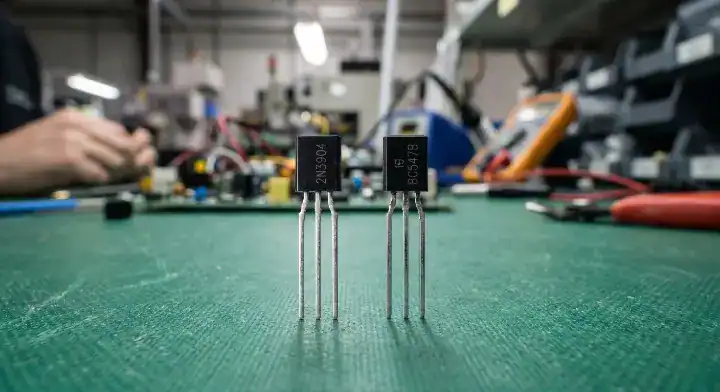
Different physical shapes dictate completely different transistor pinout sequences even for identical internal silicon dies. A 2N3904 inside a through-hole TO-92 follows an E-B-C pattern, but the exact same silicon in a surface-mount SOT-23 maps the pins entirely differently. This physical variance requires distinct routing strategies during through-hole PCB assembly compared to SMT production.
The TO-92 Standardization Problem
Users on the EDABoard Forum often ask why TO-92 packages lack a universal standard. The reality is that different regions adopted distinct manufacturing conventions, resulting in the BC547 using C-B-E while the 2N3904 uses E-B-C. Check these facts:
- There is no global standard for TO-92 pin sequences.
- European Pro Electron parts often use C-B-E.
- American JEDEC parts frequently use E-B-C.
SOT-23 vs TO-92 Pin Mapping
Transitioning a prototype from a breadboard to a printed circuit board usually involves switching from a TO-92 to an SOT-23. The pin mapping does not transfer directly, because the physical mounting style forces a layout change.
| Package Type | Mounting Style | Typical Pin 1 |
|---|---|---|
| TO-92 | Through-hole | Emitter |
| SOT-23 | Surface-mount | Base |
| TO-220 | Through-hole | Base / Gate |
Analysis: Changing a component package in your BOM requires a completely new footprint validation to prevent reversed polarity.
Key Takeaway: Never assume the pin sequence remains identical when changing package styles. Bottom line: You must verify the specific pin mapping for every individual package variant you select.
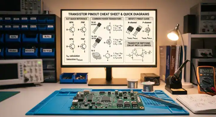
4. What Are the Exact Pin Sequences for 30+ Transistors?
Finding the exact transistor pinout for your specific component requires looking at manufacturer data rather than guessing. We compiled this master reference table to help you instantly verify the correct pin assignments for over 20 highly utilized part numbers. You must cross-reference this data with your CAD tool to prevent costly board spins.
The Master Reference Cheat Sheet
This table covers the most frequent bipolar and field-effect devices used in hardware design. For a printable version to hang above your soldering station, download our full Transistor Pinout Reference PDF. Pay attention to this list:
- It groups parts by common classifications and families.
- It highlights how identical numbers act differently in varied shells.
- It covers both through-hole and surface-mount variants.
Are You Verifying Your Specific Component?
Always use the exact Manufacturer Part Number (MPN) when ordering. A generic number will result in a random pin assignment arriving at the factory.
| Transistor | Type | Package | Pin 1 | Pin 2 | Pin 3 | Notes |
|---|---|---|---|---|---|---|
| 2N2222 | NPN | TO-18 (Metal) | Emitter | Base | Collector | Case is Collector |
| P2N2222A | NPN | TO-92 | Collector | Base | Emitter | Plastic variant |
| PN2222A | NPN | TO-92 | Emitter | Base | Collector | Different from P2N |
| 2N3904 | NPN | TO-92 | Emitter | Base | Collector | General purpose |
| MMBT3904 | NPN | SOT-23 | Base | Emitter | Collector | SMD version |
| 2N3906 | PNP | TO-92 | Emitter | Base | Collector | Complement |
| BC547 | NPN | TO-92 | Collector | Base | Emitter | Pro Electron |
| BC548 | NPN | TO-92 | Collector | Base | Emitter | 30V variant |
| BC557 | PNP | TO-92 | Collector | Base | Emitter | Complement to 547 |
| BC337 | NPN | TO-92 | Collector | Base | Emitter | 800mA rating |
| BC327 | PNP | TO-92 | Collector | Base | Emitter | Complement to 337 |
| TIP31C | NPN | TO-220 | Base | Collector | Emitter | Tab is Collector |
| TIP32C | PNP | TO-220 | Base | Collector | Emitter | Tab is Collector |
| TIP41C | NPN | TO-220 | Base | Collector | Emitter | Higher power NPN |
| TIP42C | PNP | TO-220 | Base | Collector | Emitter | Higher power PNP |
| BD139 | NPN | TO-126 | Emitter | Collector | Base | Medium power |
| BD140 | PNP | TO-126 | Emitter | Collector | Base | Medium power |
| IRF540N | N-MOSFET | TO-220 | Gate | Drain | Source | Tab is Drain |
| IRF9540N | P-MOSFET | TO-220 | Gate | Drain | Source | Tab is Drain |
| IRFZ44N | N-MOSFET | TO-220 | Gate | Drain | Source | Logic level |
| 2N7000 | N-MOSFET | TO-92 | Source | Gate | Drain | Small signal FET |
| BS170 | N-MOSFET | TO-92 | Drain | Gate | Source | Reverse of 2N7000 |
| 2N7002 | N-MOSFET | SOT-23 | Gate | Source | Drain | SMD small signal |
| IRF3205 | N-MOSFET | TO-220 | Gate | Drain | Source | High current FET |
| IRLZ44N | N-MOSFET | TO-220 | Gate | Drain | Source | Logic level drive |
Analysis: This table proves that generic part prefixes like “2N” or “BC” provide absolutely no guarantee regarding physical layout.
Key Takeaway: Identical core part numbers frequently feature swapped terminals based on their physical casing. Bottom line: Use the specific MPN suffix to define the physical layout before completing your design.
5. What Are the Key Differences in MOSFET Transistor Pinouts?
A MOSFET transistor pinout maps to Gate, Drain, and Source functions instead of the bipolar configurations. These field-effect devices operate using voltage rather than current, which means their physical terminals manage completely different electrical properties. According to the ESDA, a MOSFET gate oxide is a sensitive insulating layer typically 2–10nm thick.
Gate Oxide Sensitivity
Human body model (HBM) electrostatic discharge easily exceeds thousands of volts, destroying the gate instantly. This requires strict ESD protection protocols during handling. Keep this in mind:
- The Gate pin acts as an isolated capacitor.
- The Drain and Source conduct the heavy load.
- Static discharge ruins the ultra-thin oxide layer.
N-Channel vs P-Channel Layouts
The physical arrangement of G-D-S usually remains consistent within the same package type, regardless of channel polarity. A TO-220 IRF540N and IRF9540N both use a Gate-Drain-Source sequence from left to right.
| Package | Typical Sequence | Heatsink Tab Connection |
|---|---|---|
| TO-220 | G – D – S | Drain |
| TO-252 (DPAK) | G – D – S | Drain |
| SOT-23 | G – S – D | None |
Analysis: The metal cooling tab on high-power packages almost always connects internally to the Drain, requiring isolated mounting pads.
Key Takeaway: MOSFETs share predictable layouts within package families but demand rigorous static protection. Bottom line: You must implement grounded wrist straps and ESD-safe mats before touching any exposed MOSFET terminals.
6. How Can You Verify Unknown Parts with a Multimeter?
Verifying an unknown transistor pinout requires a high-precision digital multimeter set to diode testing mode. Users on the DIYStompboxes Forum often struggle because the Emitter-Base and Collector-Base junctions show nearly identical voltage drops. You can use our IC programming and testing services protocol to accurately identify these terminals yourself.
How Do You Find the BJT Base Pin?
The Base connects to both the Emitter and Collector via P-N junctions. You must probe all combinations until you find one pin that conducts to the other two with a ~0.7V drop. Follow these steps:
- Set your multimeter to diode test mode.
- Probe pairs until you get two valid forward voltage readings from one common pin.
- The common pin is the Base.
Distinguishing Emitter from Collector
The E-B junction features higher doping concentration, which means it exhibits a slightly higher forward voltage drop. The difference is tiny, usually only 20–50mV.
| Junction Tested | Typical Forward Voltage | Identification Meaning |
|---|---|---|
| Base to Emitter | ~0.715V | Higher reading = Emitter |
| Base to Collector | ~0.690V | Lower reading = Collector |
| Collector to Emitter | “OL” (Open Loop) | No direct connection |
Analysis: If all pin combinations display “OL” in both directions, the device is likely a MOSFET rather than a bipolar junction part.
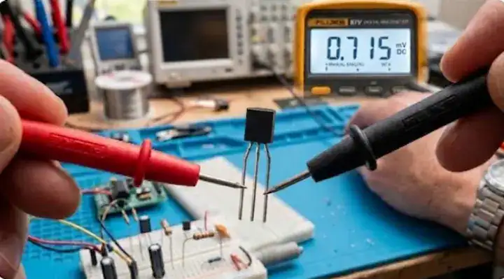
Key Takeaway: A standard multimeter can identify internal junctions if you measure the millivolt differences precisely. Bottom line: Use the junction with the slightly higher voltage reading to identify the Emitter pin.
7. Why Does the Same Part Number Have Different Lead Orders?
A generic transistor pinout can vary wildly because different semiconductor fabrication plants use proprietary lead frame designs. In our SMT production line, a client provided a BOM listing simply “2N2222”, resulting in mixed batches of TO-92 P2N2222A (E-B-C) and PN2222A (C-B-E). The second batch exhibited a 100% failure rate on functional testing because the pins were completely reversed.
The Generic Part Number Danger
Using short, generic names invites manufacturing disasters. Suppliers source parts based on availability, which means they might switch brands without warning. Here is the reality:
- “2N2222” is a generic silicon specification, not a physical layout.
- Different suffixes (P, PN, A) indicate distinct physical traits.
- Factory substitutions frequently ignore layout differences.
QueenEMS Verification Protocol
After our experience with the swapped 2N2222s, we integrated a mandatory physical verification step into our incoming quality control. We cross-reference the exact MPN against the supplied CAD data before assembly.
| Part Designation | Package | Pin Sequence |
|---|---|---|
| 2N2222 | TO-18 | E-B-C |
| P2N2222A | TO-92 | C-B-E |
| PN2222A | TO-92 | E-B-C |
Analysis: A single missing letter on a purchasing order instantly flips the component polarity and destroys the circuit.
Key Takeaway: Never trust generic numbering conventions when defining physical part dimensions. Bottom line: Always specify the full, exact alphanumeric Manufacturer Part Number on your final BOM.
8. How to Prevent Transistor Pinout Errors in BOM and PCB Design?
Catching a transistor pinout mismatch early requires aligning your CAD footprints strictly with the datasheet supplied by your specific vendor. An All About Circuits Forum user recently ruined a batch of boards because they mapped a standard 2N2222 to a P2N2222 layout. Following a strict BOM preparation guide stops these translation errors before fabrication begins.
The Manufacturer Datasheet Rule
Do not rely on generic libraries built into your design software. These libraries often contain outdated or generalized layouts that do not match modern vendor specifics. Consider these checks:
- Download the datasheet directly from the component supplier.
- Verify the exact package code matches your footprint selection.
- Confirm the 3D model aligns with the physical pads.
QueenEMS DFM Catch
A robotics startup sent us boards mapping a TO-92 “BC547” as E-B-C, but their specific ON Semiconductor parts used C-B-E. Our Free DFM engineering review flagged this mismatch immediately. We helped them update the footprint and delivered the corrected boards within 5 days, saving them $3,200.
| Step | Action Required | Risk of Skipping |
|---|---|---|
| 1 | Verify exact MPN on BOM | Wrong part ordered |
| 2 | Match datasheet to CAD library | Reversed polarity |
| 3 | Check bottom-side mirroring | Mirrored solder joints |
Analysis: Components placed on the bottom side of a PCB have their physical footprint mirrored, confusing many novice designers.

Key Takeaway: Proactive Design for Manufacturing (DFM) reviews catch library mismatches before you waste expensive silicon. Bottom line: Run a complete DFM check comparing every discrete semiconductor against its factory datasheet before manufacturing.
9. How Do Assembly Factories Catch Orientation Defects?
Verifying transistor pinout orientation during mass production relies on automated optical and X-ray systems scanning the circuit boards. The IPC-A-610 standard categorizes incorrect component orientation as a hard defect across all product classes, requiring immediate correction. We utilize advanced AOI vs X-ray vs ICT inspection systems to catch these specific placement errors instantly.
Automated Optical Inspection (AOI)
AOI machines capture high-resolution images of the populated boards before and after the reflow oven. They compare the physical component markings against the approved golden board reference. Look at these capabilities:
- AOI reads the laser-etched text on the component body.
- It verifies the position of the Pin 1 indicator dot.
- It flags parts rotated 90 or 180 degrees.
X-Ray and ICT Verification
For parts with hidden pads or symmetrical bodies, AOI might not see the error. We use 3D X-Ray inspection on complex joints and In-Circuit Testing (ICT) to verify electrical functionality.
| Inspection Tool | What It Detects | Best Used For |
|---|---|---|
| 3D AOI | Surface markings, rotation | SOT-23, TO-252 |
| X-Ray | Internal lead frames, hidden pads | QFN, BGA packages |
| ICT / Flying Probe | Junction drops, short circuits | Functional verification |
Analysis: Combining optical validation with electrical testing creates a foolproof safety net against reversed semiconductors.
Key Takeaway: Modern assembly lines rely on machine vision to verify placement accuracy at high speeds. Bottom line: Verify your PCB silkscreen clearly indicates the Emitter or Pin 1 location to help optical scanners check placement.
10. Can You Swap Devices If the Transistor Pinout Matches?
Matching a transistor pinout perfectly does not mean you can safely swap two components in a live circuit. While the physical legs might drop into the same copper holes, the internal electrical characteristics dictate whether the device will function or burn up. You must analyze the voltage ratings, current limits, and switching speeds.
Electrical Characteristic Matching
A 2N3904 and a BC548 might physically fit into identical footprint patterns if you bend the leads, but their maximum collector-emitter voltages differ significantly. Replacing a high-voltage part with a low-voltage equivalent results in immediate breakdown. Keep these parameters straight:
- Maximum Collector Current (Ic) dictates load capacity.
- Current Gain (hFE) impacts signal amplification.
- Power Dissipation (Pd) determines thermal survival.
Thermal and Frequency Limitations
Even if the DC specifications match, switching speed affects performance. A general-purpose component cannot replace a high-frequency switching transistor in an RF circuit.
| Parameter | Verification Requirement | Failure Consequence |
|---|---|---|
| Physical Layout | Must match exactly | Cannot solder to board |
| Voltage Rating | Must be equal or higher | Instant voltage breakdown |
| Current Rating | Must be equal or higher | Thermal destruction |
Analysis: Dropping an under-rated equivalent part onto a matching footprint creates a ticking time bomb under load conditions.
Key Takeaway: Physical compatibility is only the first step in finding a viable alternative component. Bottom line: You must verify that both the physical layout and the absolute maximum electrical ratings meet your circuit requirements.
FAQs
Can I use a multimeter to check if my MOSFET is damaged? Yes, you can check it using the diode mode on a digital multimeter. A healthy MOSFET will show “OL” between the Gate and Source, while a damaged gate oxide will show continuity or a very low voltage drop. Replace any part that shows a short circuit here to protect your board.
What’s the best way to determine Pin 1 on an SMT package? The most reliable method is locating the physical indicator dot or chamfered edge on the component casing. This physical mark aligns directly with Pin 1 according to JEDEC standards, which means you should always match it to the dot on your silk screen. Check your datasheet for exact marking locations before assembly.
How do I know if my TO-92 is E-B-C or C-B-E? You cannot know visually without looking up the specific Manufacturer Part Number. The TO-92 package has no global standard, resulting in identical-looking parts having completely reversed internal connections. Download the exact manufacturer datasheet before routing your board to verify.
Can I flip a transistor backwards if my PCB footprint is wrong? Yes, you can physically rotate a through-hole TO-92 by 180 degrees to correct a reversed footprint. Bending the legs crosses the Emitter and Collector, which restores functionality but looks unprofessional and stresses the metal leads. Fix the footprint in your CAD software for the next manufacturing batch.
Will an assembly house catch my reversed transistor footprint? No, not if the BOM matches the faulty Gerber files perfectly. Automated Optical Inspection only verifies that the physical part matches the orientation printed on the bare board. You must request a thorough DFM review to catch logical library errors before fabrication.
Conclusion
Verifying every single component layout saves you from catastrophic board failures and wasted production budgets. We solved the confusion surrounding unpredictable component packaging by giving you the definitive data to validate your footprints correctly. As your manufacturing partner, QueenEMS provides free DFM engineering reviews to catch these exact mismatches before they hit the assembly floor. Keep our Transistor Pinout PDF Guide saved on your desktop, and reach out and contact us today to experience a 99.7% first-pass yield on your next project. We build it right the first time, every time.
Upload your files today · Free DFM check before production · Ship worldwide
Get your PCB prototypes in as fast as 24 hours. We handle FR4, Rogers, and Flex up to 60 layers — free prototypes for 2–4 layer boards, no minimum order.
Just upload your Gerber + BOM — we source every part, assemble, and inspect (AOI + X‑Ray) so you don't have to chase suppliers. Boards ship in as fast as 24 hours.