
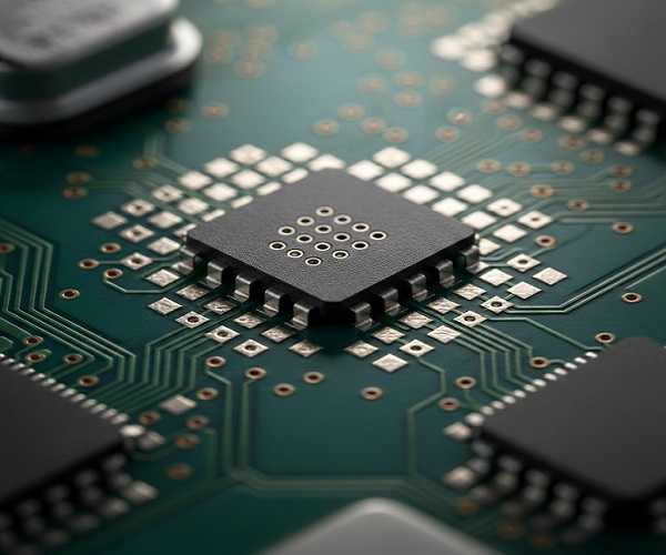
A QFN package (Quad Flat No-Lead) is a surface-mount integrated circuit carrier that connects components to printed circuit boards without traditional leads, utilizing bottom-side pads for superior thermal and electrical performance.
You are in the middle of a high-stakes product launch, and your prototypes are failing due to overheating components and signal interference in tight spaces. It is frustrating to watch your compact design suffer from thermal throttling because traditional leaded packages simply can’t dissipate heat fast enough. By switching to a high-quality qfn package, you can leverage a large exposed thermal pad and a near-zero lead inductance design to ensure your device runs cool and stable even under heavy loads.
Why is the QFN package essential for modern electronics?
The qfn package is essential because it offers a remarkably small footprint combined with excellent thermal dissipation properties required by high-power devices. By eliminating perimeter leads, this packaging style reduces the overall size and weight of the PCB while improving signal integrity.
Is the small footprint a major advantage?
Yes, the compact nature of this package allows you to maximize board real estate for other critical components. You will find that the absence of leads reduces parasitic inductance, making it ideal for high-frequency applications.
- Reduced PCB real estate usage
- Lower profile height for slim devices
- Enhanced signal speed due to shorter paths
But wait, there is more to consider regarding high-speed performance.
Key Takeaway: Using this package type allows you to build smaller, faster products without sacrificing board space.
| Feature | QFN Advantage |
| Size | Up to 60% smaller than QFP |
| Lead Inductance | Extremely Low |
| Weight | Minimal |
This data shows why space-constrained designs prioritize this format.
How does the qfn package handle heat dissipation?
A qfn package handles heat primarily through an exposed metal pad on its underside that is soldered directly to the PCB’s thermal vias. This direct path allows heat to transfer away from the silicon die much more efficiently than leaded alternatives.
What role does the thermal pad play?
The thermal pad serves as the primary cooling interface between the chip and the copper planes of your board. You must ensure proper solder coverage on this pad to avoid hot spots that could degrade component lifespan.
- Direct metal-to-PCB contact
- Reduced thermal resistance (RθJC)
- Compatibility with thermal via arrays
You might be wondering how to optimize this for your specific layout.
Key Takeaway: Proper integration of the thermal pad ensures your high-power chips remain within safe operating temperatures.
| Thermal Metric | Typical Value |
| Thermal Resistance | 20-40 °C/W |
| Pad Coverage | 50% – 80% |
Optimizing pad coverage is the secret to long-term hardware reliability.
What are the common qfn package variations?
The qfn package comes in several variations, including Thin (TQFN), Very Thin (VQFN), and Multi-Row designs, to meet different height and pin-count requirements. Choosing the right variation depends on whether you prioritize vertical clearance or maximum I/O density.
Are there differences in lead frames?
Variation in lead frame design affects how the solder fillet forms during the assembly process. You will encounter “sawn” and “punched” versions, each offering slightly different edge finishes for inspection.
- TQFN for ultra-slim mobile devices
- VQFN for standard consumer electronics
- Multi-row QFN for high pin-count logic
Think about how height constraints impact your final enclosure design.
Key Takeaway: Selecting the specific variation tailored to your enclosure height prevents mechanical interference issues.
| Variation | Typical Height |
| TQFN | 0.8 mm |
| VQFN | 0.9 mm |
| UQFN | 0.5 mm |
These dimensions allow you to select the perfect fit for slim-profile hardware.
How to optimize qfn package PCB layout?
Optimizing a qfn package layout requires precise stencil design and via placement to prevent “voiding” or component “floating” during reflow. You need to balance the amount of solder paste on the center pad to ensure a solid connection without lifting the peripheral pins.
Why is stencil aperture design critical?
The center pad stencil should be divided into a “window pane” pattern rather than one large opening. This prevents excess gas from being trapped, which creates voids that hinder thermal transfer.
- Use 50-80% solder paste coverage
- Implement 0.2mm to 0.3mm thermal vias
- Maintain proper clearance between pads
It gets even more interesting when you consider the impact of solder mask defined pads.
Key Takeaway: A segmented stencil design is the best way to ensure consistent soldering and thermal performance.
| Layout Factor | Recommendation |
| Via Pitch | 1.0 mm to 1.2 mm |
| Solder Mask | Non-Solder Mask Defined (NSMD) |
QFN Footprint Design Per IPC-7351
The IPC-7351 standard defines three density levels for QFN land patterns—Most (Level A), Nominal (Level B), and Least (Level C)—each specifying different toe, heel, and side fillet extensions. Choosing the right level depends on your assembly process: Level A provides the largest pads for hand soldering and rework, Level B suits standard reflow production, and Level C is for high-density designs where board space is critical.
When creating your QFN footprint, calculate pad dimensions using the IPC formulas that account for component tolerances, fabrication tolerances, and placement accuracy. The three key dimensions are:
- Zmax (overall pad span): Lmin + 2Jt + √(Cl² + F² + P²)
- Gmin (inner pad gap): Smax – 2Jh – √(Cs² + F² + P²)
- Xmax (pad width): Wmin + 2Js + √(Cw² + F² + P²)
The table below provides recommended footprint dimensions for the most common QFN body sizes at IPC-7351 Level B (Nominal):
| QFN Body Size | Pitch | Pad Width | Pad Length | Thermal Pad | Paste Mask (thermal) |
| 3×3 mm | 0.50 mm | 0.30 mm | 0.85 mm | 1.50×1.50 mm | 4×4 grid, 50-60% coverage |
| 4×4 mm | 0.50 mm | 0.30 mm | 0.85 mm | 2.10×2.10 mm | 4×4 grid, 50-60% coverage |
| 5×5 mm | 0.50 mm | 0.30 mm | 0.90 mm | 3.10×3.10 mm | 5×5 grid, 50-60% coverage |
| 6×6 mm | 0.50 mm | 0.30 mm | 0.95 mm | 4.10×4.10 mm | 5×5 grid, 50-60% coverage |
| 5×5 mm | 0.65 mm | 0.40 mm | 0.90 mm | 3.10×3.10 mm | 4×4 grid, 50-60% coverage |
Critical footprint design rules:
- Pad-to-pad clearance: Maintain a minimum 0.20 mm gap between adjacent terminal pads per IPC-7351 Level B. For Level C (high-density), this can be reduced to 0.15 mm, but verify your fabricator’s capability.
- Solder mask opening: Use Non-Solder Mask Defined (NSMD) pads with a 0.05–0.075 mm mask pullback from each copper pad edge. NSMD pads produce a more consistent solder fillet and are the IPC-recommended approach for QFN.
- Thermal via array: Place vias in the exposed pad area on a 1.0–1.2 mm grid with 0.25–0.30 mm drill diameter. Fill or tent these vias with solder mask to prevent solder wicking during reflow. IPC-7093 recommends limiting void coverage under the thermal pad to 50% maximum for reliable heat transfer.
- Paste mask for thermal pad: Divide the thermal pad stencil aperture into a symmetric grid pattern (e.g., 4×4 or 5×5 openings) to achieve 50–60% paste coverage. A single large opening traps flux gasses and causes voiding above 50%, which degrades thermal performance.
- Courtyard: The IPC-7351 courtyard extends 0.25 mm (Level B) beyond the package body on all sides. This keepout zone prevents component-to-component interference during pick-and-place and allows adequate clearance for rework.
What are the qfn package assembly challenges?
QFN Terminal Pad Types and Their Impact on Inspection
Not all QFN packages are created equal when it comes to solder joint visibility. The terminal pad design directly determines whether you can inspect solder fillets using standard AOI or must rely on X-ray. Understanding the three main terminal types—defined per IPC J-STD-020 and manufacturer specifications—helps you choose the right QFN variant and plan your inspection strategy accordingly.
| Terminal Type | Description | Solder Fillet | Inspection Method |
| Fully Exposed | Terminal ends extend to the package edge and are visible from the side | Partial fillet may form on the side; not guaranteed | X-ray required; limited AOI capability |
| Pull-Back | Terminal ends are recessed from the package edge by 0.05–0.10 mm | No fillet forms — solder joint is entirely hidden | X-ray mandatory; AOI cannot verify joint quality |
| Side Wettable Flank (SWF) | Terminals have a plated side surface that extends vertically, enabling solder to wick up the side | Reliable, visible solder fillet forms on the package side | Standard AOI can verify fillet; X-ray still recommended for thermal pad |
Side Wettable Flank (SWF) QFN packages are increasingly preferred for automotive and high-reliability applications because they allow solder joint inspection per IPC-A-610 Class 3 criteria without requiring X-ray on every peripheral pad. The IPC-A-610H standard (Section 8.3.8) specifies the acceptance criteria for leadless chip carrier solder joints, including minimum fillet height and wetting angle requirements.
IPC-A-610 Class 3 acceptance criteria for QFN solder joints:
| Criteria | Class 2 (Standard) | Class 3 (High-Reliability) |
| Solder fillet height (SWF terminals) | Solder wetting visible | Fillet height ≥ 25% of terminal height |
| Thermal pad voiding (max.) | ≤ 50% void area | ≤ 25% void area per IPC-7093 |
| Solder bridging between pads | Not acceptable | Not acceptable |
| Pad wetting coverage | ≥ 75% pad area wetted | ≥ 75% pad area wetted |
| Component alignment (skew) | ≤ 50% pad width overhang | ≤ 25% pad width overhang |
When specifying QFN components for your design, request SWF variants from your IC supplier whenever possible—especially for projects targeting IPC Class 3 or automotive (AEC-Q100) qualification. This eliminates the need for 100% X-ray inspection on peripheral pads, significantly reducing assembly cost and inspection time while maintaining full traceability.
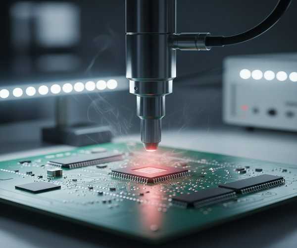
The primary challenge of qfn package assembly is the lack of visible solder joints, which makes visual inspection and manual rework difficult without specialized equipment. Since the connections are underneath the body, you cannot simply use a magnifying glass to check for bridges or opens.
Is X-ray inspection necessary?

Yes, because the leads are hidden, X-ray inspection is the only reliable way to verify the integrity of the solder joints. You must look for uniform wetting and minimal voiding under the thermal pad.
- Automated Optical Inspection (AOI) limitations
- X-ray for hidden bridge detection
- Precise pick-and-place accuracy required
You may find that standard inspection techniques just don’t cut it here.
Key Takeaway: Planning for X-ray inspection during the SMT assembly phase ensures your hidden connections are perfect.
| Challenge | Solution |
| Hidden Joints | X-Ray Inspection |
| Voids | Optimized Reflow Profile |
Advanced inspection tools are your best defense against “silent” board failures.
How does the qfn package compare to BGA?
The qfn package is often compared to BGA because both are leadless, but QFNs typically offer better thermal performance for lower pin-count devices at a lower cost. While BGAs can handle thousands of pins, QFNs excel in simplicity and power management for medium-density chips.
When should you choose QFN over BGA?
You should choose QFN when your design requires high current handling and a lower overall manufacturing cost for a simpler PCB stack-up. BGAs are better for massive I/O counts, but they often require more expensive multi-layer routing.
- Lower assembly cost for QFN
- Simpler PCB routing (fewer layers)
- Better heat dissipation for power ICs
Consider the trade-off between pin density and budget.
Key Takeaway: Use QFN for power-hungry chips with fewer pins to save on both fabrication and assembly costs.
| Metric | QFN | BGA |
| Routing Complexity | Low | High |
| Cost | Lower | Higher |
Choosing the right package early can save you thousands in production.
What are the qfn package soldering methods?
Soldering a qfn package usually involves convection reflow or vapor phase soldering to ensure even heating across the entire bottom surface. You must use a carefully controlled temperature profile to allow flux gasses to escape before the solder solidifies.
Can you manually solder a QFN?
Manual soldering is extremely difficult and generally not recommended for production, though it can be done with a hot air station and plenty of flux. You will find that a professional reflow oven provides the consistency needed for reliable bonds.
- Convection reflow for mass production
- Vapor phase for high-mass boards
- Nitrogen environment for better wetting
Have you ever wondered why some joints look dull while others shine?
Key Takeaway: Controlled reflow profiles are mandatory to achieve the high-reliability joints these packages require.
| Reflow Zone | Target Temperature |
| Preheat | 150°C – 200°C |
| Peak Reflow | 240°C – 250°C |
Precision in the oven leads to perfection on the board.
How to perform qfn package rework?
Reworking a qfn package requires a specialized rework station with bottom heating to prevent board warping and localized hot air to reflow the hidden pads. You cannot simply use a soldering iron because you cannot reach the center thermal pad or the inner lead edges.
Is bottom heating mandatory?
Absolutely, because the large copper planes attached to the thermal pad act as a heat sink, making it hard to reach reflow temperatures from the top alone. You will likely damage the board or the chip if you try to force it with only a top-side heat gun.
- Pre-heat the entire PCB
- Use precise vacuum pickup tools
- Apply fresh flux before replacement
The process is delicate, but with the right tools, it is very manageable.
Key Takeaway: Investing in a proper rework station prevents permanent damage to expensive PCB assemblies during repairs.
| Rework Step | Critical Tool |
| Removal | Hot Air + Vacuum |
| Cleaning | Solder Wick + Flux |
A careful approach to rework extends the life of your valuable prototypes.
What are the electrical benefits of the qfn package?
The qfn package provides superior electrical performance by minimizing the distance between the silicon die and the PCB, which significantly reduces parasitic capacitance and inductance. This makes it the go-to choice for high-speed RF (Radio Frequency) and high-speed digital circuits.
Does it improve signal integrity?
Yes, shorter interconnects mean less signal distortion and better EMI (Electromagnetic Interference) performance. You will notice cleaner waveforms and less cross-talk compared to leaded packages like SOIC or QFP.
- Minimal bond wire length
- Low lead-to-lead capacitance
- Improved ground plane connection
Imagine the performance gains in your next wireless communication module.
Key Takeaway: For RF and high-speed data, this package minimizes noise and maximizes signal clarity.
| Electrical Property | QFN Performance |
| Inductance | < 1 nH |
| Frequency Range | Up to 20+ GHz |
Low inductance is the key to unlocking true high-speed potential.
How to choose a reliable qfn package manufacturer?
Choosing a qfn package assembly partner involves verifying their X-ray capabilities, reflow profile expertise, and history with fine-pitch components. You need a factory that understands the nuances of stencil tension and paste chemistry to avoid common assembly pitfalls.
What certifications should you look for?
You should look for ISO 9001 and IPC-A-610 Class 3 compliance to ensure the factory maintains the strict tolerances required for leadless assembly. Ask about their experience with moisture-sensitive devices (MSD) to ensure your chips don’t “popcorn” during reflow.
- In-house 3D X-ray inspection
- Solder paste inspection (SPI) systems
- Climate-controlled component storage
Are you ready to take your assembly quality to the next level?
Key Takeaway: Partnering with a factory that uses SPI and X-ray ensures your production run is defect-free from the start.
| Service Check | Importance |
| 3D X-Ray | Mandatory |
| SPI | Highly Recommended |
The right partner turns complex assembly into a seamless production flow.
Conclusion
Mastering the qfn package is a game-changer for engineers aiming to build high-performance, compact electronics. We have explored how its thermal pad solves overheating issues, how its leadless design boosts signal integrity, and the critical layout techniques needed to avoid assembly defects. By addressing these thermal and electrical challenges, you can confidently integrate these components into your most demanding projects.
At Queen EMS, we specialize in overcoming the complexities of fine-pitch assembly and thermal management. Whether you need help with DFM optimization or high-reliability production, we are here to ensure your designs succeed. Contact us today to discuss your next project and see how our expertise can bring your vision to life. We don’t just assemble boards; we build the future of reliable electronics together.
FAQ
Can I manually inspect QFN solder joints? No, because the pads are under the package. You must use X-ray inspection to see the internal solder wetting and check for bridges or voids.
What is the best way to prevent QFN voiding? The best way is to use a “window pane” stencil design for the thermal pad. This allows gasses to escape during reflow, significantly reducing void formation.
How do I know if my QFN is overheating? Check your thermal via design and solder coverage. If the center pad isn’t 60-80% soldered to a good ground plane, the chip will likely throttle or fail under load.
Can I use QFN for high-voltage applications? It is possible, but you must be careful. The tight spacing between pads means you need to check creepage and clearance requirements for your specific voltage levels.
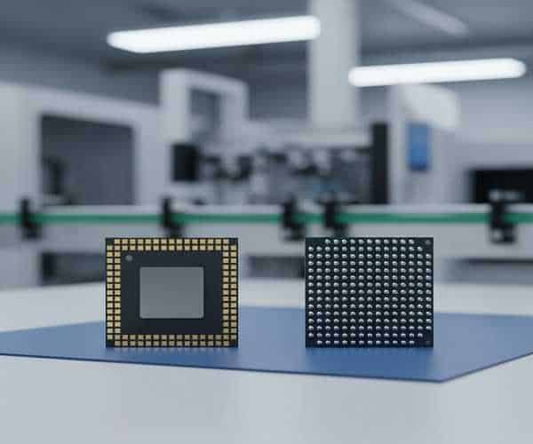
What is the difference between QFN and DFN packages? QFN (Quad Flat No-Lead) has terminal pads on all four sides of the package, while DFN (Dual Flat No-Lead) has pads on only two sides. QFN supports higher pin counts and typically offers better thermal performance due to its larger exposed pad and quad-sided heat distribution. Choose DFN for simple, low-pin-count devices like voltage regulators; choose QFN when you need more I/O connections or better heat dissipation for microcontrollers, RF ICs, or power management chips.
What is the difference between QFN and QFP packages? QFP (Quad Flat Package) has visible leads extending from all four sides, while QFN is leadless with pads on the bottom surface. QFN is up to 60% smaller than an equivalent QFP, has significantly lower lead inductance (under 1 nH vs. 3–5 nH for QFP), and provides better thermal performance through its exposed pad. However, QFP is easier to hand-solder and visually inspect, making it preferable for prototyping or low-volume rework scenarios where X-ray inspection is not available.
What does the QFN exposed pad connect to? The exposed thermal pad on the bottom of a QFN package is typically connected to ground (GND) or left as a dedicated thermal connection — always refer to the IC manufacturer’s datasheet for the specific requirement. On the PCB side, solder the exposed pad to a copper pad connected to an internal ground plane through an array of thermal vias (0.25–0.30 mm drill, 1.0–1.2 mm pitch). This provides both electrical grounding and efficient heat dissipation from the die to the board.
What is a wettable flank QFN package? A wettable flank (also called Side Wettable Flank or SWF) QFN has plated terminal surfaces that extend up the side of the package body. During reflow, solder wicks up these side surfaces to form a visible fillet — similar to a traditional leaded package. This allows standard AOI equipment to verify solder joint quality without X-ray, which is why wettable flank QFNs are increasingly required in automotive (AEC-Q100) and medical applications where 100% optical inspection is mandatory.
What stencil thickness should I use for QFN assembly? For standard QFN packages with 0.50 mm pitch, use a 0.125 mm (5 mil) thick stencil. For fine-pitch QFN at 0.40 mm pitch, step down to 0.100 mm (4 mil) in the QFN area using a step stencil. The thermal pad aperture should be divided into a window-pane grid pattern targeting 50–60% paste coverage — a single large opening causes excessive voiding and may float the component during reflow. Maintain an area ratio above 0.66 for all peripheral pad apertures to ensure consistent paste release.
How do I handle QFN moisture sensitivity during assembly? Most QFN packages are rated MSL 3 (Moisture Sensitivity Level 3) per IPC/JEDEC J-STD-020, meaning they must be reflowed within 168 hours of exposure to ambient conditions after opening the dry pack. If this floor life is exceeded, bake the components at 125°C for 24 hours (or per the manufacturer’s datasheet) before assembly. Failure to manage moisture properly can cause “popcorn cracking” — internal steam pressure during reflow that delaminates the die from the lead frame, resulting in immediate or latent field failures.