

An annular ring explained by a PCB manufacturer is simply the copper pad area left around a drilled hole. You spend weeks perfecting your board layout, only to have the factory reject it due to clearance issues. This frustrating delay ruins your project timeline and inflates your budget. Fortunately, understanding and optimizing your annular ring specifications before submitting your Gerber files guarantees a seamless manufacturing process. To jump directly to practical solutions, you can explore the IPC-6012 standards or our via type specs.
Contents
- What is an annular ring in a PCB?
- How do you calculate the minimum annular ring?
- What causes tangency and breakout in an annular ring?
- How does drill wander affect your annular ring?
- Mechanical vs laser drill: Which annular ring is best?
- When should you add teardrops to your annular ring?
- What are the IPC-6012 standards for your annular ring?
- How does IPC-2221 define minimum annular ring sizes?
- What are the best annular ring specs by via type?
- How to set DRC rules for your annular ring?
What is an annular ring in a PCB?
It is the remaining copper pad area surrounding a drilled hole on a printed circuit board. Understanding the annular ring is crucial because it creates the electrical connection between the via and the copper traces. If this copper ring is too thin, the connection might fail during soldering or operation.
How does the via structure work?
A standard via consists of the pad, the drilled hole, and the copper plating. Here is the deal: The ring is what anchors your component leads and ensures conductivity.
- Copper pad diameter
- Finished hole size
- Drill bit tolerance
Why is this copper ring critical?
It absorbs the thermal stress during the wave soldering or reflow process.
| Feature | Function | Consequence of Failure |
|---|---|---|
| Copper Pad | Conducts signal | Open circuit |
| Plated Wall | Layer transition | Signal loss |
This table illustrates how each structural element relies on the copper ring for survival.
Key Takeaway: Always ensure you allocate sufficient pad area around your vias to prevent catastrophic connectivity failures during the assembly process.
How do you calculate the minimum annular ring?

You calculate it using the formula: (Pad Diameter – Hole Diameter) / 2. This standard formula helps you determine the exact width of your annular ring before fabrication. By accurately calculating this value, you avoid spacing violations that trigger factory holds. It ensures your design translates perfectly into physical hardware.
What is the standard formula breakdown?
Let’s dive in: You must thoroughly understand the variables inside the math.
- Pad Diameter: The total width of the copper circle
- Hole Diameter: The size of the actual drill bit used
- Division by two: Accounts for both sides of the hole
How does a real-world calculation look?
If you have a 30 mil pad and a 10 mil drill hole, the calculation is (30 – 10) / 2. This gives you a 10 mil ring width.
| Variable | Example Value | Result |
|---|---|---|
| Pad Size | 30 mil | N/A |
| Drill Hole | 10 mil | N/A |
| Ring Width | N/A | 10 mil |
These numbers demonstrate how a seemingly large pad can yield a surprisingly narrow ring.
Key Takeaway: Always verify your calculated ring width against your manufacturer’s specific capabilities to prevent costly production delays.
What causes tangency and breakout in an annular ring?
Tangency and breakout occur when the drill bit wanders off the center of the copper pad. A perfect annular ring is difficult to achieve because mechanical drills inherently vibrate and drift during operation. When the hole touches the edge, it is tangency; when it breaches the edge, it is breakout.
Are tangency defects acceptable?
You might be wondering: Is this acceptable? It depends entirely on your target IPC class requirements.
- Hole edge touches pad edge
- No copper breach occurs
- Acceptable for Class 1 and some Class 2
What are the dangers of breakout?
Breakout is a severe defect where the drill hole completely breaches the copper pad perimeter. This severely compromises the structural integrity of the via and the connection.
| Defect Type | Description | Reliability Risk |
|---|---|---|
| Tangency | Hole touches pad edge | Medium |
| Breakout | Hole breaches pad edge | High |
| Perfect Centering | Hole in exact center | Zero |
This defect matrix shows why drill precision is fundamentally critical to board longevity.
Key Takeaway: Design your pad sizes with enough buffer margin to safely absorb normal manufacturing tolerances without causing a breakout.
How does drill wander affect your annular ring?
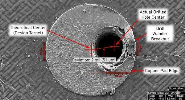
Drill wander shifts the hole off-center, directly shrinking the available copper width on one side. Even advanced factory machines experience some level of drill wander, which constantly threatens your annular ring integrity. If the wander exceeds your designed buffer, the via connection will inevitably fail.
What are typical tolerance levels?
What’s the real story? You cannot physically eliminate machine vibration completely.
- Spindle runout variations
- Material density shifting the bit
- Stack-up thickness issues
How should you compensate for drift?
To compensate, designers must artificially inflate the pad size beyond the mathematical minimum. Most standard PCB manufacturers require an allowance for a 2 mil to 3 mil drill wander.
| Drill Wander | Required Buffer | Pad Increase |
|---|---|---|
| 1 mil | Low | +2 mils |
| 2 mils | Medium | +4 mils |
| 3 mils | High | +6 mils |
This adjustment chart highlights the exact compensation values needed to counteract mechanical drill drift effectively.
This is a frequently misunderstood issue because designers assume the annular ring is measured the same way on all layers. It is not. On external layers, the annular ring is measured from the edge of the finished plated hole wall to the edge of the pad. On internal layers, the annular ring is measured from the edge of the raw drilled hole (before plating) to the edge of the pad. Since the raw drill hole is larger than the finished plated hole by twice the plating thickness (typically 1.0 mil per side for Class 3), the internal layer measurement starts from a larger hole diameter. This means your internal layer annular ring is inherently smaller than your external layer ring for the same pad size. Additionally, inner layers suffer more from lamination registration shift, which adds another 1–2 mils of tolerance stackup that external layers do not experience. The practical fix is to increase your internal layer pad sizes by 2–4 mils compared to external layer pads, or use a uniform pad size that accommodates the worst-case internal layer tolerance. Ask your fabricator for their specific internal layer registration capability before finalizing your design.
Key Takeaway: Always assume a minimum of 2 mils of drill wander and increase your pad diameters accordingly to protect your design.
Mechanical vs laser drill: Which annular ring is best?
Laser drills offer extreme precision, allowing for significantly smaller ring widths compared to mechanical drills. A mechanical drill requires a larger annular ring because physical drill bits vibrate and wander more than focused light. Choosing the right drilling method dictates your entire high-density layout strategy.
What are mechanical drilling limits?
Here is the kicker: It is perfect for standard through-holes but struggles with miniaturization.
- Cost-effective for standard boards
- Prone to physical vibration
- Requires larger pad sizes
Why choose laser drilling?
Laser drilling enables micro-vias with a tiny 2 mil ring requirement. This technology is absolutely essential for modern high-density interconnect designs.
| Drill Type | Min Ring Width | Primary Application |
|---|---|---|
| Mechanical | 3 mil | Standard Through-Hole |
| Laser | 2 mil | HDI Micro-vias |
| Backdrill | 4 mil | High-speed Signal |
This technology comparison clearly demonstrates why laser precision is mandatory for dense HDI circuit layouts.
Aspect ratio, defined as the ratio of board thickness to drilled hole diameter, directly impacts annular ring reliability because higher aspect ratios cause more drill wander and via barrel stress. The industry standard maximum aspect ratio for reliable mechanical drilling is 10:1. For a standard 1.6mm board, this means your minimum drill size should be 0.15mm (6 mil). For a thick 3.2mm board, the minimum drill increases to 0.32mm (12.6 mil). When you are forced to use small drills in thick boards (exceeding 10:1 ratio), drill wander increases significantly, sometimes exceeding 3–4 mils, which directly eats into your annular ring budget. At aspect ratios above 12:1, you should expect to increase your pad sizes by an additional 3–4 mils beyond standard recommendations to compensate for the increased wander. For designs requiring small holes in thick boards (such as high-layer-count backplanes), consider laser drilling for blind vias on the outer layers combined with larger mechanically drilled through-holes for the full stackup. This hybrid drilling approach lets you maintain tight annular rings on the surface layers while using more forgiving tolerances for the deep through-holes.
Key Takeaway: Upgrade to laser drilling capabilities when your design density forces your via pad geometries below standard mechanical limits.
When should you add teardrops to your annular ring?
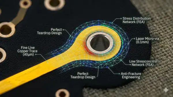
You should use teardrops when connecting thin traces to vias to prevent trace detachment during drill wander. Adding teardrops fortifies the junction between the trace and your annular ring against extreme mechanical and thermal stress. This simple design trick significantly boosts your overall manufacturing yield rate.
How does the teardrop mechanism work?
Picture this: It acts like a structural bridge reinforcing a weak joint.
- Prevents trace-to-pad cracking
- Reduces thermal stress concentration
- Mitigates breakout risks
What are ideal application scenarios?
They are highly recommended for any trace thinner than 5 mils entering a via. They are also vital for flexible printed circuits that endure constant bending.
| Scenario | Teardrop Required? | Benefit |
|---|---|---|
| < 5 mil trace | Yes | Prevents detachment |
| Flex PCB | Yes | Absorbs bending stress |
| Standard rigid | Optional | Improves yield |
This application matrix outlines exactly when adding extra copper reinforcement is a non-negotiable design rule.
Key Takeaway: Enable automated teardrop generation in your EDA software to drastically reduce the risk of trace severance near your vias.
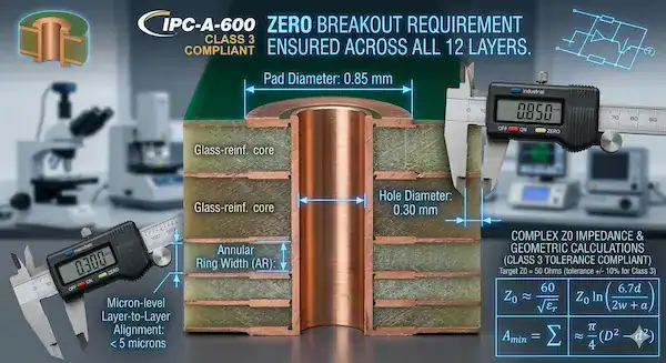
What are the IPC-6012 standards for your annular ring?
IPC-6012 sets the strict acceptance criteria for via integrity across three distinct product classes. Your target IPC class dictates exactly how much annular ring breakout is legally permissible for your specific product. Designing blindly without these standards guarantees inspection failures.
What are Class 1 and Class 2 rules?
Now let’s get down to business: Class 2 allows 90-degree breakout, provided the connection remains functional.
- Class 1: Allows 90-degree breakout
- Class 2: Breakout allowed with conditions
- Used for non-critical electronics
What are Class 3 critical requirements?
Class 3 covers high-reliability medical and aerospace products. It strictly demands a complete, unbroken ring with zero breakout allowed under any circumstances.
| IPC Class | Breakout Allowed? | Minimum Ring Width |
|---|---|---|
| Class 1 | Yes (90 degrees) | Not fully critical |
| Class 2 | Yes (with limits) | > 1 mil |
| Class 3 | No (Zero breakout) | > 2 mil |
This standard breakdown proves that high-reliability aerospace products demand flawless pad geometries without exception.
This is the classic clash between IPC Class 3 annular ring requirements and modern fine-pitch BGA routing. Class 3 demands a minimum 2 mil annular ring with zero breakout, which for an 8 mil drill hole means a 24 mil pad diameter (including fabrication allowance). At 0.8mm BGA pitch (31.5 mils), after subtracting the BGA pad and the via pad with required clearances, there is virtually no room left to route even a 4 mil trace between vias. Three proven solutions exist. First, use teardrop-shaped via pads instead of circular pads. Teardrops provide the required copper margin at the trace-to-pad junction while reducing the pad footprint in the routing channel direction, freeing approximately 2–3 mils of additional routing space. Second, use laser-drilled microvias with a 4 mil drill, which allows a much smaller pad size (12–14 mil) compared to mechanical drills. Third, consider via-in-pad technology where the via is placed directly inside the BGA pad, completely eliminating the need to route between separate via pads. Via-in-pad requires filled and planarized vias, adding fabrication cost, but it is the most routing-efficient solution for pitches below 0.8mm.
Key Takeaway: Always verify your product’s target IPC class before setting your internal DRC rules to avoid catastrophic compliance failures.
How does IPC-2221 define minimum annular ring sizes?
IPC-2221 provides the master mathematical formula: Min Land Size = Min Hole Size + 2 times Min Annular Ring plus Fabrication Allowance. This comprehensive equation ensures your annular ring survives the harsh realities of physical factory production. It forces you to account for actual manufacturing tolerances, not just ideal geometry.
How do you understand the formula?
This is where it gets interesting: Producibility Levels A, B, and C dictate this allowance.
- Level A: General design complexity
- Level B: Moderate design complexity
- Level C: High design complexity
How do you apply producibility levels?
If you select Level C, you must assume a tighter fabrication allowance for high-density boards. This means your calculated pad size must be extremely precise to succeed.
| Producibility Level | Complexity | Fabrication Allowance |
|---|---|---|
| Level A | Low | Largest |
| Level B | Moderate | Standard |
| Level C | High | Tighter |
This complexity chart reveals how pushing technological limits forces you to calculate tighter manufacturing margins.
Key Takeaway: Always consult your chosen manufacturer to confirm their true fabrication allowance before finalizing your pad calculations.
What are the best annular ring specs by via type?
Through-hole vias need 5 mils, blind vias need 4 mils, and micro-vias require 2 mils. Matching the correct annular ring to the specific via type is fundamental for an optimal layout. Using a one-size-fits-all approach guarantees a bloated, inefficient circuit design.
What are standard through-hole specs?
Truth be told: you must give them at least 5 mils to survive wave soldering.
- Plated Through-Hole: > 5 mil
- Component Hole: > 7 mil
- High mechanical stress areas
What are blind and micro-via specs?
Blind vias sit inside the board and require around 4 mils. Micro-vias, processed with lasers, can safely operate with a tiny 2 mil width.
| Via Type | Recommended Minimum | Technology Used |
|---|---|---|
| Through-Hole | 5 mils | Mechanical Drill |
| Blind Via | 4 mils | Controlled Depth |
| Micro-via | 2 mils | Laser Drill |
This specification table serves as a direct reference guide for setting up your initial layout parameters.
Key Takeaway: Categorize your vias correctly in your design software to apply the tightest possible parameters without violating safety margins.
How to set DRC rules for your annular ring?
You set DRC rules by entering your manufacturer’s minimum pad-to-hole clearance values into your software’s design rule manager. Configuring your EDA software to automatically monitor your annular ring prevents manual checking errors. It acts as an automated safety net before you ever generate your final Gerber files.
How to configure Altium Designer?
Believe it or not: setting this up takes less than two minutes.
- Open Design Rules Editor
- Select Routing Via Style
- Input minimum hole and pad sizes
What is the vital pre-Gerber checklist?
Before exporting files, run a final batch DRC specifically targeting via clearances. This 5-step checklist acts as your ultimate defense against factory rejection.
| Checklist Step | Action Required | Goal |
|---|---|---|
| Step 1 | Verify IPC Class | Define tolerance |
| Step 2 | Input manufacturer limits | Sync with factory |
| Step 3 | Run automated DRC | Catch visual errors |
This software verification table highlights the exact sequence required to lock down your via geometries flawlessly.
The confusion arises because IPC specifies the minimum acceptable annular ring after fabrication (what’s left on the finished board), while your EDA tool’s DRC value needs to account for all manufacturing tolerances that will erode the ring during production. The IPC Class 2 minimum of 1 mil is what the inspector measures on the final board. But to reliably achieve that 1 mil after accounting for drill wander (±2 mils typical), lamination registration shift (±1.5 mils), and imaging tolerances (±0.5 mils), your design must start with a significantly larger ring. Your fabricator’s recommendation of 3.5 mils is their calculated design minimum that accounts for their specific equipment tolerances. Always use your fabricator’s recommended value, not the IPC minimum, as your DRC setting. A practical approach: set your DRC annular ring to 4 mils for standard boards, 5 mils for boards over 8 layers (more lamination shift), and 3 mils only if your fabricator explicitly confirms their registration capability supports it. For Class 3 boards, add an additional 1–2 mils above these values.
Key Takeaway: Never skip the final automated design rule check, as it guarantees your layout matches the physical capabilities of your assembly partner.
Conclusion
This comprehensive guide resolved the complexities surrounding via pad design, proving that precise calculations prevent catastrophic assembly failures. We provide 2-hour quotations, rigorous DFM reviews, and expert engineering support to ensure your layouts transition flawlessly into physical products. QueenEMS is committed to elevating your manufacturing experience through transparency, precision, and relentless quality control. For expert assistance on your next project, please contact us today to experience true engineering excellence.
FAQ
Q1: Can I use a 1 mil width for standard through-hole vias? No. A 1 mil width is far too thin for mechanical drills and will almost certainly result in severe breakout during fabrication.
Q2: What’s the best way to prevent trace detachment near a via? Using teardrops is the absolute best method. Teardrops add structural copper mass to the junction, preventing the trace from cracking under thermal stress.
Q3: How do I know if my design requires IPC Class 3 standards? You must determine your product’s end-use environment. If you are building life-critical medical devices or aerospace hardware, Class 3 is legally mandated.
Q4: Can I trust software default settings for pad clearances? No. Default software settings are generic and rarely align with the specific fabrication allowances of your chosen manufacturing factory.
Q5: What’s the most reliable drill technology for HDI micro-vias? Laser drilling is the absolute most reliable option. It offers extreme precision, enabling the safe production of 2 mil widths required for high-density boards.