
The material known as prepreg is a dielectric insulator made of woven fiberglass impregnated with partially cured epoxy resin. Are unpredictable impedance drifts and catastrophic delamination issues ruining your expensive multilayer assemblies? Unpredictable dielectric thickness often causes these severe signal integrity failures during final bare board testing. By selecting the correct prepreg materials, you can eliminate impedance variations and guarantee absolute long-term reliability for your critical projects.
- What Is Prepreg And Why Is It Critical In Multilayer PCBs?
- How Is Prepreg Manufactured For PCB Fabrication?
- What Are The Different Prepreg Types And Glass Styles?
- How Does Resin Content Affect Prepreg Performance?
- What Is The Difference Between Prepreg And Core In PCBs?
- How Does Prepreg Thickness Impact Your Stackup Design?
- How Does Prepreg Selection Affect Impedance Accuracy?
- What Happens To Prepreg During The Lamination Process?
- What Common Prepreg Mistakes Cause Costly PCB Failures?
- How To Specify Prepreg Correctly In Your PCB Docs?
1. What Is Prepreg And Why Is It Critical In Multilayer PCBs?
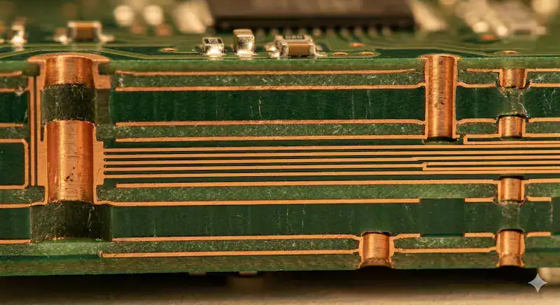
The fundamental component called prepreg acts as the critical bonding agent that firmly holds your entire multilayer circuit board together. This specialized insulating layer transforms from a semi-solid state into a flowing liquid during the intense heat of the lamination press. Without this highly engineered bonding sheet, fabricating complex electronics with internal copper routing would remain physically impossible. It dictates the final dielectric distance between conductive copper layers definitively.
Why Is Prepreg Essential For Complex Stackups?
This versatile composite material provides essential electrical isolation while simultaneously acting as the structural foundation for your electronic components. You might be wondering. How does it influence the final electrical performance of the circuit? It establishes the exact dielectric baseline necessary for calculating precise controlled impedance traces on high-speed digital designs.
- It fills the empty microscopic gaps between etched copper patterns seamlessly.
- It strictly defines the distance between signal layers and reference planes.
- It provides the necessary mechanical rigidity for the assembled bare board.
Key Takeaway: Understanding this fundamental insulating layer empowers designers to build significantly more reliable and electrically stable circuit boards.
| Feature Category | Core Functionality | Impact On Manufacturing |
|---|---|---|
| Structural Integrity | Binds adjacent FR4 layers | Prevents severe delamination |
| Electrical Isolation | Separates internal copper paths | Stops catastrophic short circuits |
| Dielectric Spacing | Controls exact layer distances | Ensures accurate signal impedance |
Evaluating these core functionalities reveals why selecting the optimal bonding sheet is absolutely vital for manufacturing success.
2. How Is Prepreg Manufactured For PCB Fabrication?
The intricate manufacturing process for prepreg involves impregnating woven fiberglass fabrics with specialized liquid epoxy resin formulations under strict environmental controls. Huge industrial rollers pull the raw glass fabric through massive vats containing precisely mixed liquid chemical resin solutions. The coated fabric then passes through towering heating ovens that partially cure the sticky epoxy into a manageable solid state. This exact B-stage curing phase ensures the material remains perfectly stable for extended storage before final lamination.
Can You Explain The Curing Phase?
The careful thermal treatment stops the chemical reaction prematurely, creating a dry sheet that will liquefy again when heated later. Here is the deal. If the factory bakes the material too long, it will never melt properly during the final board pressing stage. Our engineering-driven agile manufacturing pipeline conducts rigorous incoming material inspections to verify optimal resin flow parameters automatically.
- Glass weaving establishes the mechanical strength of the underlying fabric.
- Resin impregnation saturates every microscopic void within the glass bundles.
- B-stage heating locks the chemical structure into a suspended semi-cured state.
Key Takeaway: The precise control of the B-stage thermal curing cycle dictates the ultimate bonding strength of your multilayer boards.
| Manufacturing Step | Technical Action | Quality Assurance Metric |
|---|---|---|
| Glass Weaving | Interlocking fine fiberglass yarns | Uniform physical fabric tension |
| Resin Coating | Submerging fabric in liquid epoxy | Consistent total resin absorption |
| Thermal Baking | Pausing the epoxy chemical reaction | Exact B-stage curing verification |
Monitoring these manufacturing tolerances tightly guarantees that every sheet behaves predictably during the final intense lamination pressing cycle.
3. What Are The Different Prepreg Types And Glass Styles?
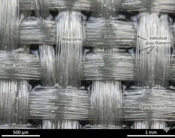
Different types of prepreg are defined by their specific fiberglass weave styles, which directly determine their nominal physical thickness and structural rigidity. The industry relies heavily on standard commercial designations like 106, 1080, 2116, and 7628 to identify these various glass fabric structures quickly. A 106 style utilizes extremely fine glass yarns resulting in a remarkably thin sheet, while a 7628 style uses heavy yarns for massive thickness. Engineers must carefully combine these distinct weave styles to achieve the exact target dielectric thickness required for the design.
How Do Weave Styles Affect Fabrication?
The physical geometry of the woven glass directly influences how effectively the liquid resin can flow and fill internal copper gaps. What is the real story? Thicker glass styles provide superior structural stability but contain less proportional resin volume available for flowing into deep crevices.
- The 106 style is exceptionally thin and perfectly suited for high-density interconnects.
- The 2116 style serves as a reliable medium-thickness standard across most fabricators.
- The 7628 style delivers maximum structural rigidity and rapid thickness accumulation.
Key Takeaway: Selecting the appropriate glass weave style balances your required dielectric thickness against the necessary mechanical strength of the board.
| Glass Weave Style | Relative Nominal Thickness | Typical Application Scenario |
|---|---|---|
| 106 | Very Thin (~2.0 mils) | High-density microvia HDI designs |
| 1080 | Thin (~2.5 mils) | Standard multilayer signal separation |
| 7628 | Thick (~7.0 mils) | Rapid core building and rigidity |
Understanding these distinct fabric geometries helps designers assemble functional multilayer structures without causing unnecessary manufacturing bottlenecks.
4. How Does Resin Content Affect Prepreg Performance?
The specific resin content within your prepreg fundamentally dictates its ability to successfully encapsulate heavy internal copper traces during lamination. Manufacturers classify these materials into standard resin (SR), medium resin (MR), and high resin (HR) categories based on their exact chemical volume percentages. When you design boards with highly dense inner copper patterns, you absolutely need high resin options to prevent microscopic air voids. Insufficient resin volume leaves deep etched channels partially empty, which eventually leads to catastrophic delamination under high thermal stress.
Why Is Resin Volume Crucial?
The available epoxy must physically displace all trapped atmospheric air while securely bonding the adjacent fiberglass layers together flawlessly. This is where it gets interesting. The ratio between the glass matrix and the epoxy directly alters the final dielectric constant of the pressed composite material.
- Standard resin (SR) sits around 40% and suits continuous uniform copper planes.
- Medium resin (MR) hovers near 50% providing balanced flow characteristics.
- High resin (HR) exceeds 60% and successfully fills extremely aggressive copper etching.
Key Takeaway: Matching your chosen resin content to the density of your internal copper layers prevents disastrous manufacturing voids entirely.
| Resin Classification | Volume Percentage | Best Production Use Case |
|---|---|---|
| Standard Resin (SR) | 40% to 50% | Solid continuous copper reference planes |
| Medium Resin (MR) | 50% to 60% | Mixed signal routing and ground planes |
| High Resin (HR) | Greater than 60% | Heavy copper traces with deep empty gaps |
Calculating the correct chemical volume percentage ensures structural perfection while simultaneously maintaining strict electrical impedance targets accurately.
5. What Is The Difference Between Prepreg And Core In PCBs?

A core is a fully cured rigid FR4 laminate clad with copper on both sides, while prepreg is an uncured B-stage bonding sheet. Understanding this fundamental distinction prevents catastrophic multilayer alignment failures because the two materials behave entirely differently inside the pressing machine. In a typical 6-layer board, you utilize two central cores, three intermediate bonding sheets, and two external raw copper foils. The absolute outer layers of a standard stackup must always utilize uncured bonding sheets to adhere to the external copper foils correctly.
How Do Their Properties Contrast?
The dielectric constant of a cured core remains virtually permanent, whereas the uncured bonding sheet fluctuates slightly during the final heat pressing. Ready for the good part? You cannot build a standard foil-build multilayer architecture if you mistakenly place a hard core on the absolute outer boundary.
- Cores deliver mechanical rigidity and possess completely hardened internal resin structures.
- Bonding sheets melt dynamically to encapsulate the etched internal copper features completely.
- Outer layers absolutely require B-stage resin to grip the smooth outer copper foils.
Key Takeaway: Differentiating between fully cured laminates and dynamic bonding sheets is mandatory for engineering a successful multilayer stackup correctly.
| Material Type | Curing Status | Copper Cladding |
|---|---|---|
| Standard Core | Fully Cured (C-stage) | Copper clad on both top and bottom |
| Bonding Sheet | Partially Cured (B-stage) | No copper cladding initially |
| Outer Foil | Pure Metallic Copper | Requires B-stage resin for strong adhesion |
Properly sequencing these distinct materials guarantees that your complex multilayer assemblies withstand severe mechanical and thermal environmental testing.
6. How Does Prepreg Thickness Impact Your Stackup Design?
The final pressed thickness of your prepreg drops significantly below its nominal datasheet value because flowing resin must fill empty copper gaps. A client insisted on calculating their 1.6mm stackup using nominal data without accounting for the sparse 35% copper density on layer two. The final pressed board ended up at 1.48mm, causing their precision-machined rigid mechanical enclosure to rattle aggressively during vibration testing. We now enforce a proprietary resin-flow calculation algorithm during our free DFM review for every single multilayer order we process.
How Should You Calculate Dimensions?
The final dimensional measurement depends entirely on how much liquid epoxy gets squeezed into the etched valleys of your internal layout. You might be wondering. How can you accurately predict the final physical dimensions of a standard 1.6mm four-layer circuit board? The combined dielectric distance of the cores and bonding sheets usually measures around 1.4mm to accommodate the outer copper plating.
- Flowing epoxy naturally reduces the nominal distance between your conductive signal layers.
- Dense copper planes absorb very little liquid resin during the lamination cycle.
- Sparse routing layouts demand massive resin volumes, shrinking the dielectric thickness significantly.
Key Takeaway: Never rely on raw datasheet dimensions; always utilize specialized manufacturing software to calculate post-pressing thickness adjustments accurately.
| Stackup Variable | Impact On Final Thickness | Engineering Compensation Strategy |
|---|---|---|
| Dense Copper Planes | Minimal thickness reduction | Standard nominal calculations remain mostly valid |
| Sparse Routing Lines | Extreme thickness reduction | Require additional resin volume or extra sheets |
| Heavy 3oz Copper | Massive thickness unpredictability | Demand proprietary factory flow calculation models |
Our adjusted stackup engineering approach has maintained our stellar 99.7% first-pass yield rate across thousands of custom electronic batches.
7. How Does Prepreg Selection Affect Impedance Accuracy?
Your selected prepreg directly alters signal impedance because the dielectric constant fluctuates based on precise resin content and specific glass styles. An aerospace client experienced a massive 12ps/inch skew on a 5GHz differential pair using standard 1080 woven glass fabric. The high-speed signals were crossing different sparse fiberglass bundles unevenly, creating chaotic microscopic variations in the local dielectric constant. We transitioned their critical design to a spread glass 1080S configuration while keeping the identical FR4 material family completely unchanged.
Why Does Fiber Weave Matter?
The alternating physical pattern of glass bundles and epoxy pools creates an inconsistent electrical environment for extremely fast traveling electromagnetic waves. This is where it gets interesting. Shifting the resin content from 42% to 56% can drastically change the dielectric constant by nearly 5% overall.
- High resin volumes generally lower the overall dielectric constant of the composite material.
- Standard open weaves cause differential pairs to experience severe timing synchronization mismatch.
- Spread glass styles flatten the woven bundles, creating a perfectly homogenous electrical medium.
Key Takeaway: Always demand empirical measured dielectric data from your fabricator instead of trusting generic marketing numbers from raw material datasheets.
| Material Characteristic | Effect On High-Speed Signals | Recommended Design Action |
|---|---|---|
| Open Glass Weave | High timing skew (>10ps/inch) | Unacceptable for speeds exceeding 2GHz |
| Spread Glass Weave | Minimal timing skew (~1ps/inch) | Mandatory for modern high-speed differential pairs |
| Variable Resin Content | Unpredictable impedance shifts | Use factory-validated empirical Dk measurements |
The skew dropped to just 1.2ps/inch instantly, leading our engineering matrix to strictly mandate spread glass styles for high-speed digital designs.
8. What Happens To Prepreg During The Lamination Process?
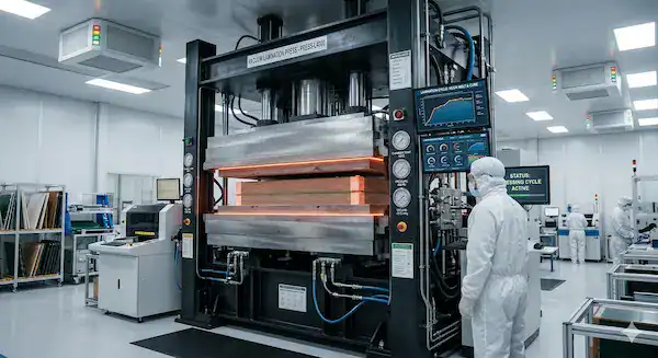
During the intense vacuum lamination process, the semi-solid prepreg undergoes a spectacular chemical transformation from a sticky solid into a flowing liquid. The massive hydraulic presses apply tremendous physical pressure while simultaneously ramping up the internal temperature to exceed 350 degrees Fahrenheit. This intense thermal energy dramatically lowers the viscosity of the epoxy, forcing it to violently flow into every microscopic etched copper crevice. Once the maximum temperature threshold is achieved, the chemical cross-linking accelerates rapidly, permanently hardening the entire composite structure into a rigid block.
Can You Describe The Viscosity Curve?
The material hits a specific thermal point where its resistance to flowing drops to absolute zero, known as the melt viscosity minimum. What is the real story? If the hydraulic pressure engages too late, the epoxy will gel prematurely and fail to encapsulate the copper.
- Heat transforms the dormant B-stage epoxy into an aggressive flowing liquid state.
- Sustained high temperatures trigger an irreversible chemical polymerization cross-linking chain reaction.
- Cooling cycles lock the internal mechanical stresses, creating a stable C-stage laminate permanently.
Key Takeaway: The flawless execution of the thermal and pressure lamination profile separates premium factory capabilities from unreliable discount manufacturing brokers.
| Lamination Phase | Epoxy Physical State | Critical Processing Action |
|---|---|---|
| Initial Heating | Softening solid | Careful vacuum application to remove trapped air |
| Melt Viscosity Min | Flowing liquid | Maximum hydraulic pressure to fill copper gaps |
| Final Curing | Hardened solid | Sustained peak temperature to finalize polymerization |
Mastering these complex thermodynamic transitions guarantees that your finished circuit boards will survive extreme environmental testing without suffering from delamination.
9. What Common Prepreg Mistakes Cause Costly PCB Failures?
The most common prepreg mistake involves using inadequate resin volume to fill thick inner-layer copper channels, leading to severe voids. Designers frequently underestimate how much liquid resin gets violently absorbed by heavy copper etching during the intense hydraulic pressing cycle. We had a customer submit an 8-layer stackup specifying three sheets of thin 106 material between two heavy 2oz copper layers. During lamination, the ultra-thin resin couldn’t fill the deep etch channels, resulting in disastrous structural voids across 30% of cross-sections.
Why Are Stackup Limitations Crucial?
Stacking more than three consecutive bonding sheets creates extreme manufacturing risks for severe resin voids and dangerous fiberglass measling defects. Ready for the good part? When your design requires an interlayer spacing exceeding 15 mils, you must insert a dummy core instead of piling up raw sheets.
- Thick copper layers drastically increase the total physical thickness of the fabricated board.
- High-resin (HR) materials aggressively prevent air voids within heavy copper routing gaps.
- Dummy cores stabilize extremely thick dielectric spacing requirements safely and highly reliably.
Key Takeaway: Always collaborate with your fabrication partner to mathematically validate available resin volume against your specific internal copper distribution density.
| Design Mistake | Manufacturing Consequence | Engineering Solution |
|---|---|---|
| >3 Prepreg Sheets | Measling and layer slippage | Insert a fully cured dummy FR4 core |
| Thin Resin + 3oz Cu | Massive structural voids | Utilize 7628 High Resin (HR) materials |
| Ignoring Cu Density | Incorrect final board thickness | Request a free factory DFM flow calculation |
We switched them to a single sheet of 7628 HR material, dropping the void rate to zero and passing 6x reflow safely.
10. How To Specify Prepreg Correctly In Your PCB Docs?

You should specify overall thickness, core dimensions, and target impedance, letting the manufacturer optimize the exact prepreg sheets required. Designers who stubbornly lock in specific material part numbers often face massive production delays and significantly increased raw material costs. Our senior engineering matrix strongly recommends labeling the bonding layers simply as “as needed to meet impedance and overall thickness requirements.” This intelligent documentation approach allows our factory floor to tune the dielectric spacing dynamically based on our real-time empirical material measurements.
How To Avoid Supply Chain Delays?
Demanding obscure or highly exotic fiberglass styles practically guarantees that your rapid prototyping project will suffer from devastating material sourcing delays. Here is the deal. Selecting widely stocked standard materials like 1080, 2116, or 7628 prevents unnecessary supply chain bottlenecks entirely while maintaining excellent performance.
- Specifying exact part numbers forces factories to order expensive custom material batches slowly.
- Allowing factory-level material optimization guarantees the fastest possible quick-turn manufacturing turnaround times.
- Mixing different material brands within one stackup almost always causes catastrophic thermal delamination.
Key Takeaway: Trusting your manufacturing partner to select the optimal bonding sheets based on your electrical requirements yields the best production results.
| Documentation Strategy | Fabrication Result | Impact On Lead Time |
|---|---|---|
| Locking Exact Part Numbers | Forces custom material procurement | Significant delays (weeks) |
| Mixing Different Brands | Causes thermal expansion mismatch | Board failure during assembly |
| Allowing Factory Optimization | Enables immediate stock utilization | Ultra-fast turnaround (24 hours) |
Granting your fabrication partner the flexibility to choose the appropriate bonding sheets ensures you receive a highly reliable, perfectly tuned product.
Mastering the complexities of fiberglass weaves, resin content, and pressed thickness is the ultimate secret to designing highly reliable multilayer circuit boards. By understanding how these specialized bonding sheets actually behave under immense heat and pressure, you can prevent catastrophic impedance drifts and eliminate frustrating manufacturing delays permanently. We proudly offer full turnkey services, up to 60-layer fabrication capabilities, and rigorous 3D AOI inspections to ensure your complex stackups succeed flawlessly. If you are ready to stop guessing about dielectric tolerances and start building perfect boards, contact us today. Our engineering-driven agile manufacturing pipeline delivers transparent, data-driven excellence, transforming your intricate designs into dependable reality.
FAQ
Q1: What is the fundamental difference between prepreg and a core? A core is a fully cured rigid FR4 laminate clad with copper, while the bonding sheet remains in an uncured B-stage state. The bonding sheet melts during lamination to act as the glue binding the rigid cores together.
Q2: How does the resin content impact my heavy copper designs? Heavy copper etching leaves deep empty channels that demand massive liquid resin volumes to fill properly. You must utilize High Resin (HR) materials to completely encapsulate 2oz or 3oz copper without creating destructive internal air voids.
Q3: Can I stack four or five sheets together to get a thicker dielectric? No, stacking more than three consecutive sheets causes unpredictable layer slippage and severe measling defects during pressing. If you need a massive dielectric gap exceeding 15 mils, you must insert a fully cured dummy core instead.
Q4: Why did my final board thickness come out thinner than my software predicted? Your software likely calculated the nominal datasheet thickness without accounting for the flowing resin filling your sparse internal copper patterns. The liquid epoxy gets squeezed into the empty etched valleys, reducing the final physical distance between the adjacent layers significantly.
Q5: What is the best way to handle impedance control in my fabrication notes? You should clearly state your target impedance, reference layers, and trace widths, but leave the exact bonding sheet selection open. Adding a note like “adjust prepreg as needed to meet impedance” allows the factory to use their precise empirical measurements.