
Quick Answer: PCB via current capacity depends on three factors: drill diameter, copper plating thickness, and your allowable temperature rise. A standard 0.3mm drill via with 20µm copper plating (IPC Class 2) can safely carry approximately 0.8–1.0A with a 10°C temperature rise. For high-current applications, use parallel vias — to carry 10A, you typically need 10–13 standard vias (0.3mm) or 5–7 larger vias (0.5mm) placed symmetrically around the pad. The via is often the bottleneck in high-current paths: widening your trace but keeping a single small via means the via limits your entire current capacity. Always check that your via current rating matches or exceeds your trace current rating for the same temperature rise target.
Key takeaways:
- A 0.3mm drill via (20µm plating, 10°C rise) carries ~0.8–1.0A; a 0.5mm drill carries ~1.5–2.0A
- To carry 10A, use 10–13 standard 0.3mm vias or 5–7 larger 0.5mm vias in parallel
- Add 50% safety margin on via count — parallel via current distribution is never perfectly equal
- IPC Class 3 plating (25µm min) gives 25% more current capacity than Class 2 (20µm) for the same drill size
- The via is almost always the weakest link if you have only one via in a high-current trace path
- Specify “IPC-6012 Class 3 via plating: 25µm minimum” in fab notes for high-reliability high-current designs
Table of Contents
- How Does a Via Actually Carry Current — and Why Is It Different from a Trace?
- The PCB Via Current Capacity Reference Table: What Each Via Size Can Actually Handle
- How Many Vias Do You Need to Carry 5A, 10A, or 20A?
- Is the Via Always the Weakest Point in Your High-Current Path?
- How Does Thermal Relief Affect PCB Via Current Capacity?
- Does Via Plating Thickness Actually Matter — and How Do You Specify It?
- Should You Use Tented, Plugged, or Filled Vias for High-Current Paths?
- The PCB Via Current Capacity Design Checklist: What to Verify Before You Send Your Gerbers
- Frequently Asked Questions
You’ve routed heavy power traces for your new board, expecting it to handle 10A effortlessly. But during field testing, the board randomly resets under load, and a cross-section reveals cracked via barrels that caused microscopic open circuits. After processing over 2,400 assembly orders last year, we’ve seen this specific failure play out hundreds of times. Engineers widen their traces meticulously but completely ignore their pcb via current capacity, turning microscopic layer transitions into massive thermal bottlenecks. Let’s break down exactly how much power a single via can take, why parallel vias act unpredictably, and how to properly specify them before manufacturing starts.
How Does a Via Actually Carry Current — and Why Is It Different from a Trace?
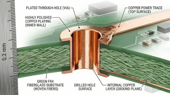
A via carries current exclusively through the cylindrical copper plating on its barrel wall, and a standard 0.3mm via with 20µm plating handles about 0.8–1.0A for a 10°C rise. Unlike surface traces exposed to open air, vias are trapped inside FR4 fiberglass, meaning they retain heat and have a 20–30% lower current rating than a surface trace with the exact same cross-sectional area.
The factory floor reality is… many designers treat vias just like tiny traces. They are not. The physics of how they dissipate heat changes everything. According to the IPC-2152 standard, which replaced the outdated IPC-2221B, calculating via capacity requires looking at three exact variables: your drill diameter, the actual copper plating thickness, and your target temperature rise.
When you push power through a board, the cross-sectional area of that thin copper cylinder dictates your absolute limit. You can calculate this effective area using the formula: π × drill diameter × copper plating thickness. Understanding your baseline PCB copper weight guide helps set expectations, but remember that via plating is an independent process from your base foil weight.
- Outer traces shed heat efficiently through convection into the surrounding air
- Vias are thermally insulated by the surrounding dielectric substrate
- A 10°C or 20°C temperature rise is the standard safety limit for most consumer and industrial designs
- Thermal vias are a completely different application — designed specifically to conduct heat away from components, not to carry electrical current
The PCB Via Current Capacity Reference Table: What Each Via Size Can Actually Handle
To determine your pcb via current capacity quickly, refer to our baseline metric: a 0.2mm signal via carries ~0.5A, a standard 0.3mm via handles ~0.9A, and a larger 0.5mm via supports ~1.7A (assuming standard 20µm plating and a 10°C temperature rise).
So what does this actually mean for your layout? You stop guessing. Instead of using blind rules of thumb from old engineering forums, you use hard data to size your transitions. Below is the reference table that most competitors fail to provide, mapping exact drill sizes to realistic current limits.
Table A: Via Current Capacity Reference (IPC Class 2 Standard Plating, 20µm)
| Drill Diameter | Finished Hole Size (Approx.) | Plated Copper Area | Current Capacity (10°C Rise) | Current Capacity (20°C Rise) | Typical Application |
|---|---|---|---|---|---|
| 0.20mm (8mil) | ~0.16mm | ~10mil² | ~0.5A | ~0.7A | Signal vias, very low current |
| 0.25mm (10mil) | ~0.21mm | ~13mil² | ~0.7A | ~1.0A | Low power signals |
| 0.30mm (12mil) | ~0.26mm | ~16mil² | ~0.9A | ~1.3A | Standard signals / light power |
| 0.40mm (16mil) | ~0.36mm | ~21mil² | ~1.3A | ~1.8A | Medium power transitions |
| 0.50mm (20mil) | ~0.46mm | ~27mil² | ~1.7A | ~2.4A | Heavy power transitions |
| 0.60mm (24mil) | ~0.56mm | ~33mil² | ~2.1A | ~3.0A | High-current applications |
| 0.80mm (32mil) | ~0.76mm | ~43mil² | ~2.8A | ~4.0A | Heavy power loads, requires large drill |
Note: The above figures are based on the IPC-2152 standard, 1.6mm board thickness, FR4 substrate, and standard 20µm copper plating. Actual values may vary by ±20% depending on factory processes, plating uniformity, and board thickness. IPC Class 3 copper plating (25µm) can increase current capacity by approximately 25% over these base values.
If you are designing tight, high-density boards, balancing hole sizes becomes an economic decision. Microvias take up less space but restrict power flow heavily. You can review our HDI PCB cost guide to understand when to pay for laser-drilled microvias versus simply increasing your standard mechanical drill sizes for better power delivery.
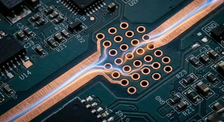
How Many Vias Do You Need to Carry 5A, 10A, or 20A?
To safely carry 10A across a layer transition, you need 10 to 13 standard 0.3mm vias, or 5 to 7 larger 0.5mm vias, factoring in a 10°C temperature rise. You must always add a 50% safety margin to your via count because parallel vias never share current equally, with the via closest to the current source taking the heaviest load.
Pull back the curtain on this… Engineers constantly ask on Reddit and EEVblog: “I need to carry 10A through a layer transition. How many vias do I need and what size?” The math seems simple. If one 0.3mm via handles ~0.9A, then eleven should handle 10A perfectly.
But electricity behaves like water in pipes. It takes the path of least resistance. The first via it encounters will carry significantly more current than the fifth via in the array. If you only provide the bare minimum number of holes, that first via will overheat, slowly degrading its copper wall until it cracks. Once it fails, the second via takes the brunt, creating a cascading failure.
Table B: Parallel Via Count Reference (0.3mm Drill, 20µm Plating, 10°C Temp Rise Limit)
| Target Current | Calculated Vias Needed | Recommended Actual Vias (50% Margin) | Symmetrical Layout Suggestion |
|---|---|---|---|
| 1A | 1–2 | 2 | 2 placed symmetrically |
| 2A | 2–3 | 4 | 2×2 square grid |
| 5A | 5–7 | 8–10 | 4×2 or circular arrangement |
| 10A | 10–13 | 15–18 | 3×5 or dense circular arrangement |
| 20A | 20–25 | 30+ | Dense multi-row array, consider larger drill |
Note: Current distribution in parallel vias is unequal; vias closest to the current inlet carry a heavier load. A symmetrical layout and a 50% safety margin are strongly recommended. For currents exceeding 20A, prioritize switching to larger drill sizes (0.5mm+) to reduce the total via count.
- Choose 0.4mm or 0.5mm vias for arrays rather than stacking dozens of tiny 0.2mm vias, as larger holes plate much more uniformly.
- Arrange your via arrays symmetrically around the component pad instead of stacking them all on one side.
- For extreme power requirements exceeding 20A, standard FR4 designs reach their limits. Review heavy copper PCB design strategies and partner with a capable heavy copper PCB manufacturing facility to handle massive thermal loads.
Is the Via Always the Weakest Point in Your High-Current Path?
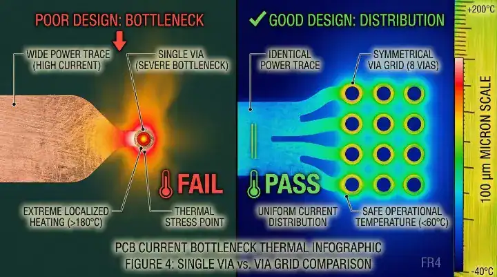
Yes, if you widen a trace to handle 5A but use only one standard 0.3mm via, that single via becomes a severe 1A bottleneck for your entire circuit. The pcb via current capacity must always match or exceed the current rating of the traces it connects.
Now, here is what typically happens… You will see this question pop up constantly on AllAboutCircuits: “I widened my traces to handle 5A but I only have one standard via for the layer transition. Is the via now my bottleneck?” Absolutely. A wide trace leading into a tiny hole is like a six-lane highway merging into a dirt road.
You cannot spot this error easily during functional testing. A standard via won’t instantly blow up like a fuse. Instead, it creates localized heating. Over time, thermal cycling causes the barrel copper to crack. To fix this, you must apply the same temperature rise limits to your vias that you apply to your traces. Learn how to calculate the surface copper side in our PCB trace width and current capacity guide.
Factory Floor Reality: > Problem: 80% of power supply layouts we receive contain at least one via bottleneck. The most common error: transitioning a 2oz power plane through two standard 12mil vias. Solution: We run an automated DFM check on every board, flagging any layer transition where the total via cross-sectional area falls below 80% of the connecting trace area. Result: This simple engineering review step cuts thermal-related field failures to zero for our OEM clients.
How Does Thermal Relief Affect PCB Via Current Capacity?
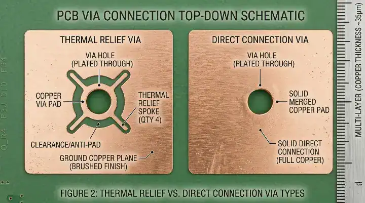
Using standard thermal reliefs on a power via reduces its current carrying capacity by up to 60% because you replace a solid 360-degree copper connection with two or four thin copper spokes. For high-current layer transitions exceeding 2A, you must use solid direct connections to the power plane to avoid catastrophic localized heating.
That said… thermal reliefs exist for a reason. EDA software applies them automatically to inner planes to prevent the copper from acting like a massive heatsink during the soldering process, which could lead to cold joints. However, a via used purely for a layer transition does not have a component leg soldered into it.
When you apply a thermal relief to a transition via, you throttle the current through microscopic copper spokes. If your layout requires navigating heavy currents through planes, always select “direct connect” or “solid” for your via connections. You can read more about managing plane connections safely in our PCB copper pour vs ground plane design rules.
- Thermal reliefs restrict current flow and increase electrical resistance at the junction.
- Plated through-holes (PTH) holding component pins require thermal reliefs for assembly yield.
- Layer-transition vias (stitching vias) require solid connections for maximum power transfer.
Does Via Plating Thickness Actually Matter — and How Do You Specify It?
Copper plating thickness directly controls your via’s cross-sectional area; upgrading from 20µm to 25µm plating increases your current capacity by a linear 25%. To guarantee this, you must explicitly write “Via plating per IPC-6012 Class 3: minimum 25µm copper in via barrel” in your fabrication notes.
So what does this actually mean for your budget? Many engineers assume all manufacturers provide the exact same barrel thickness. They don’t.
Under the default IPC-6012 Class 2 standard, factories only need to provide an average of 20µm of copper in the hole, with an absolute minimum allowed drop to 15µm. In a high-current application, a 15µm wall drastically reduces your thermal limits. If your design demands high reliability under heavy loads, you cannot just write “good plating” on your drawing. You need to understand actual PCB fabrication tolerances and pay for precision.
- Specify Class 3 specifically for the via plating if you want the 25µm minimum guarantee.
- Request a cross-section report with your first article inspection to verify the actual barrel thickness under a microscope.
- Remember that asking for thicker surface copper (like 2oz or 3oz) does not automatically mean the factory will plate the via walls thicker.
Should You Use Tented, Plugged, or Filled Vias for High-Current Paths?
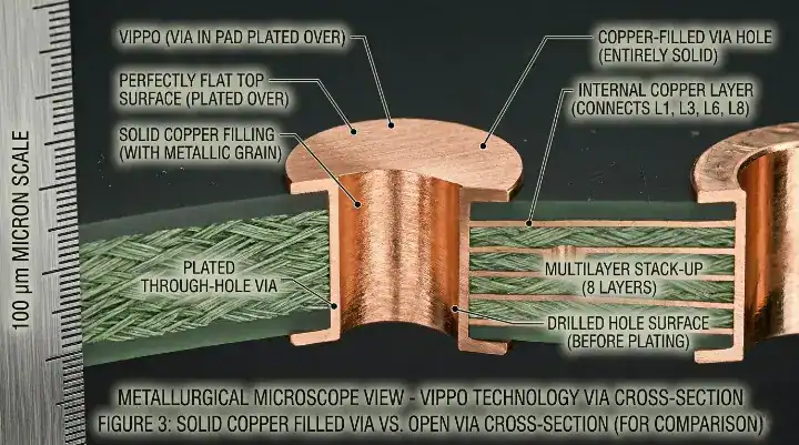
Standard via tenting does not increase your PCB via current capacity, but using copper-filled microvias or silver-epoxy filled vias can improve thermal dissipation by roughly 15-20%. However, standard non-conductive epoxy filling offers zero electrical benefit and is strictly used to prevent solder wicking under components.
The real question is… are you paying for a via treatment expecting it to solve a current bottleneck? Many designers select “plugged vias” thinking the extra epoxy adds physical durability under high electrical loads.
Tenting simply covers the via with solder mask. Plugging fills it with non-conductive epoxy. Neither adds conductive mass. If you place a via directly under a high-power MOSFET (via-in-pad), you must use conductive filling and plating over it (VIPPO) to handle the extreme heat and current. Check our complete breakdown on PCB via tenting vs plugging vs filling to align your fabrication requests with your thermal goals.
- Tenting (solder mask) provides environmental protection but zero current capacity increase.
- Non-conductive epoxy plugging prevents solder wicking during assembly.
- Conductive filling (copper/silver) slightly boosts thermal transfer but is expensive.
- If you need more current, adding more standard parallel vias is always cheaper than specifying conductively filled vias.
The PCB Via Current Capacity Design Checklist: What to Verify Before You Send Your Gerbers
Before finalizing your high-current board, verify that every layer transition has a 50% extra via count, parallel vias are placed symmetrically, and you use solid connections without thermal reliefs. Missing these checks guarantees thermal bottlenecks under peak loads.
Here is exactly how you verify this… human error happens. The best way to catch a mismatched trace and via is a hard checklist. Run your design against these specific parameters before generating your final fabrication files.
Checklist: High-Current Via Design Verification
| Verification Item | Standard | Consequence of Failure |
|---|---|---|
| Does single via capacity meet requirements? | Check reference table; use 10°C rise as target | Single via overload causes localized overheating |
| Is there a 50% safety margin on via count? | Actual count = Calculated need × 1.5 | Unequal current distribution overloads some vias |
| Are parallel vias arranged symmetrically? | Distributed symmetrically around pad, avoid one-sided stacking | Vias nearest the inlet become overloaded |
| Is via plating thickness specified in fab notes? | High-current designs must state “IPC-6012 Class 3: 25µm min” | Factory defaults to Class 2 (20µm), which may be insufficient |
| Is the via the bottleneck of the path? | Via capacity ≥ connected trace capacity | Wide trace + tiny via = via is the bottleneck |
| Are thermal reliefs avoided for layer transitions? | High-current vias must use solid connections, avoid thermal reliefs | Thermal reliefs increase resistance and exacerbate heating |
| Are filled/capped vias required? | Consider VIPPO for high current + BGA pad flatness needs | Hollow vias experience higher thermal stress under heavy load |
Designing a high-current board? Tell us your current requirements and we will verify your via sizing and plating spec before we quote. Upload your Gerbers for a free DFM check — we flag via current bottlenecks and insufficient parallel via counts before production starts, saving you from field failures under high load.
Frequently Asked Questions
Can I just use one massive via instead of several smaller ones? It depends. While a single large via (like 1.0mm) can carry heavy current, it introduces soldering risks during assembly. Solder can wick down a large open hole, starving the component pad. It is usually better to use an array of 0.4mm or 0.5mm vias. Upload your layout to us if you need help balancing thermal mass and assembly safety.
How do I know if my vias are failing under load? Look for localized discoloration on your PCB mask directly over the layer transitions. If the FR4 turns slightly brown, your via is acting like a heating element. To prove it definitively, you must cross-section the board and check for micro-cracks in the copper plating.
Does filling a via with epoxy increase its current capacity? No. Non-conductive epoxy filling does absolutely nothing for electrical current capacity. Even conductive epoxy has far higher resistance than pure plated copper. If you need more current, you need more plated copper — either through thicker barrel walls (Class 3) or more parallel holes.
Will 2oz surface copper give me thicker via walls? No, surface foil weight and via plating thickness are independent processes. You can start with 2oz base copper and the factory might still only plate 20µm in the holes. You must specify via barrel thickness separately in your fabrication notes. Request a free engineering review today to lock down your fab notes.
Written by the QueenEMS Engineering Team. Ready to build your next board with verified high-current reliability? Contact us today.