
Quick Answer: Proper pcb design for test (DFT) requires adding dedicated test points and access structures during layout so automated equipment can verify your assembly. Skipping DFT and trying to add it after layout costs $5,000–$15,000 in redesigns and custom fixtures — roughly 100x more than spending two hours on test point placement early on. The core decision is ICT vs flying probe: flying probe requires no fixture (ideal for prototypes under 200 boards), while ICT fixtures cost $3,000–$8,000 upfront but drop per-board test costs to $1–$3, making ICT mathematically cheaper at production volumes above 200–300 units.
Key takeaways:
- DFT review must happen at 50% layout completion — not after routing is done.
- ICT fixtures cost $3,000–$8,000 upfront; flying probe costs $15–$25 per board with no fixture.
- Break-even between flying probe and ICT is typically 200–300 boards depending on complexity.
- Test points must be 1.27mm (50mil) minimum diameter, 2.54mm (100mil) center-to-center spacing for ICT.
- Bottom-side-only test points reduce fixture cost by 40%–60% compared to dual-sided access.
- For dense HDI boards: JTAG boundary scan + flying probe + functional testing replaces full ICT coverage.
Table of Contents
- What Is PCB Design for Test — and Why Does It Have to Start at Layout, Not After?
- What Happens to Your Production Cost When You Skip DFT During Layout?
- At What Production Volume Does ICT Actually Pay For Itself?
- What Are the Non-Negotiable Test Point Design Rules for ICT and Flying Probe?
- How Do You Handle PCB Design for Test on a Dense HDI Board Where Test Points Won’t Fit?
- The DFT Checklist: What to Verify at 50% Layout Completion
You just finalized your 8-layer board layout, exported the Gerbers, and sent them to your contract manufacturer for a production quote. Three days later, the engineering team replies: “This board has zero test point access under the BGAs. We cannot run In-Circuit Testing (ICT). You either need to pay $12,000 for a custom functional jig or spend three weeks redesigning the board.” After reviewing thousands of layouts, we see this massive mistake weekly. Good pcb design for test is not an optional layout preference; it is a strict financial calculation that dictates your manufacturing yield and unit cost. Here is how to build a testable board from the ground up.
What Is PCB Design for Test — and Why Does It Have to Start at Layout, Not After?
PCB design for testability (DFT) is the deliberate process of adding physical access points, strategic vias, and spacing rules into your layout so factory machines can physically touch and measure the electrical integrity of your assembled board. You must implement DFT when your layout is roughly 50% complete, because adding test points after 100% routing forces you to rip up and reroute thousands of traces.
The factory floor reality is… engineers often treat testing as a post-production afterthought. They assume the factory will magically figure out how to verify the components. The reality is that testing hardware requires physical copper to touch. Proper DFM for PCB design ensures your board can be manufactured, but DFT ensures we can actually prove it works. However, we must be transparent: DFT is not a magic shield against all failures. Even with 100% ICT coverage, PCBA testing and field failure prevention still requires a layer of functional testing, because ICT verifies physical solder joints, not firmware behavior or high-speed signal integrity.
What Happens to Your Production Cost When You Skip DFT During Layout?
Skipping DFT forces you into three highly expensive recovery options: paying a $12–$22 premium per board for slow flying probe tests, spending $2,000–$5,000 to completely redesign your PCB layout, or investing $8,000–$15,000 in a custom functional test jig. None of these options are cheap, and all of them delay your market launch by weeks.
Engineers frequently face this crisis: “We finished layout without thinking about DFT. Now our EMS says the board is basically untestable with ICT. What are our options and how much will this cost us?” If you are running a batch of 500 boards, relying on a flying probe test (because you lack test points for an ICT bed-of-nails) will cost you an extra $10,000 in machine time alone. We mandate a DFT review on every order precisely because we saw a medical device client lose $12,000 and three weeks of lead time building a custom mechanical jig just because they forgot to route BGA signals to bottom-side test pads.
Pull back the curtain on this… * Option 1: Flying Probe Penalty. Slows production down massively. Adds roughly $15 per board.
- Option 2: Layout Redesign. Costs $2k-$5k in engineering time and delays production by 2-3 weeks.
- Option 3: Custom Functional Jig. Costs up to $15k and requires 4-8 weeks to design and machine.
- The Solution: Spend 2 hours adding test points at the 50% layout phase.
At What Production Volume Does ICT Actually Pay For Itself?
In-Circuit Testing (ICT) pays for itself and becomes cheaper than flying probe testing when your production volume crosses the 200 to 300 board threshold. You calculate this break-even point by dividing your upfront ICT fixture cost by the difference between the flying probe per-board cost and the ICT per-board cost.
Startups regularly ask us: “We are starting production at 100 boards per month. Should we invest in ICT fixtures now or stick with flying probe?” The math holds the answer. Let’s assume a medium-complexity 6-layer board. The custom bed-of-nails ICT fixture costs $5,000. Testing via flying probe costs $20 per board (including program amortization), while ICT takes only 45 seconds and costs $2 per board.
Break-even Formula: Break-even volume = ICT fixture cost ÷ (Flying probe cost per board - ICT cost per board)
$5,000 ÷ ($20 - $2) = 278 boards. On board number 279, ICT becomes the cheaper strategy.
| Comparison Metric | ICT (Bed of Nails) | Flying Probe | Decision Recommendation |
|---|---|---|---|
| Fixture Cost | $3,000–$8,000 (Custom per design) | $0 (No hard fixture) | Flying probe wins for prototypes. |
| Per-Board Test Cost | $1–$3 / board | $15–$25 / board | ICT wins massively at high volume. |
| Test Time | 30–90 seconds / board | 15–30 minutes / board | ICT is 15-30x faster for mass production. |
| Break-Even Volume | Approx. 200–300 boards | Better below 200 boards | Base your choice purely on expected volume. |
| Design Flexibility | Poor (Requires new fixture if layout changes) | Excellent (Just update the software) | Stick to flying probe if design is unstable. |
| DFT Requirements | Strict (Needs dedicated >1mm test points) | Flexible (Can touch component pins) | ICT demands strict layout discipline. |
| Defect Detection | 85%–95% (With good layout) | 60%–80% (Limited by probe access) | ICT provides superior physical coverage. |
Not sure whether ICT or flying probe is right for your production volume? Send us your board specs and we will run the break-even calculation for your specific design.
What Are the Non-Negotiable Test Point Design Rules for ICT and Flying Probe?
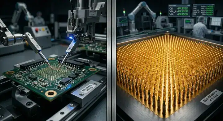
To build a reliable ICT fixture, your test points must be a minimum of 1.0mm (40mil) in diameter — ideally 1.27mm (50mil) — and spaced at least 2.54mm (100mil) apart from center to center. You must also place them strictly on the bottom side of the PCB whenever possible, as a single-sided ICT fixture costs 40% to 60% less than a dual-sided clam-shell fixture.
Ignoring these physical rules guarantees your test fixture will suffer from false failures. If test points are too close together, the mechanical pogo pins inside the fixture will short out or physically break. Furthermore, you must provide the factory with accurate alignment features. We need at least two non-plated through holes (NPTH) placed diagonally across the board, measuring exactly 3.2mm (125mil) in diameter, to physically lock the board onto the fixture. Understanding your PCB fabrication tolerances ensures these tooling holes do not drift during manufacturing.
So what does this mean at the production line?
- Edge Clearance: Keep all test points at least 3.2mm (125mil) away from the board edge to allow the fixture vacuum seal to grip the PCB.
- Component Clearance: Maintain a 2mm keep-out zone around tall components so the probe heads do not crash into capacitors.
- Via Usage: Instead of placing test points on the top layer, drop a via and place the pad on the bottom layer to avoid paying for a top-side probe plate.
How Do You Handle PCB Design for Test on a Dense HDI Board Where Test Points Won’t Fit?

When BGA pitches drop below 0.5mm on dense HDI boards, you cannot physically fit test points; you must replace mechanical ICT coverage with a combination of JTAG boundary scan testing, selective flying probe access, and rigorous functional testing. Forcing physical test points into a high-density layout destroys your signal integrity and bloats your board size.
Designers of complex systems often panic: “My board is so dense with BGAs that I cannot fit enough test points for ICT coverage. What is my testing strategy?” First, push whatever signals you can to the bottom layer. Good BGA pad design and escape routing usually leaves open areas on the bottom of the board for probe access. Second, utilize chips that support JTAG. Boundary scan can electronically verify the connections between complex ICs without a single physical test point, instantly boosting your test coverage from 50% to over 75%.
That said… you must accept that 100% ICT coverage is impossible on HDI.
- For dense BGA assembly service, rely on 3D X-ray to verify the physical solder joints.
- Use flying probes to touch exposed component pins on the perimeter of the dense zones.
- Implement a robust functional testing EVT DVT PVT protocol to validate the system as a whole rather than testing every single net.
The DFT Checklist: What to Verify at 50% Layout Completion
Run your layout through this checklist when your routing is halfway complete. Catching a blocked net now takes thirty seconds to fix; finding it after the board is manufactured requires a $5,000 fixture redesign.
Upload your layout files at 50% completion — our DFT review will flag any test coverage gaps before they become expensive fixture redesigns.
| Checklist Item | Standard Requirement | Consequence if Ignored |
|---|---|---|
| Net Coverage | At least 1 test point per net (more for power rails) | Uncovered nets cannot be electrically verified by ICT. |
| Test Point Diameter | ICT: 1.0mm min, 1.27mm ideal. Flying probe: 0.5mm min. | Probe miss rate skyrockets to 5%–10%, causing false failures. |
| Test Point Spacing | Center-to-center distance ≥ 2.54mm (100mil) | Pogo pins physically collide and break inside the fixture. |
| Bottom Side Preference | >90% of test points should live on the bottom layer | Dual-sided fixtures cost 60%–80% more than single-sided. |
| Edge Clearance | Minimum 3.2mm (125mil) from PCB edge | Fixture hold-down clamps will cover the test pads. |
| Component Clearance | Keep-out zone of 2mm from tall components | Probes will crash into parts and damage the PCBA. |
| BGA Under-Routing | Route critical nets via dog-bone to open bottom areas | BGA nets become physically un-testable by probes. |
| Tooling Holes | 2x NPTH, 3.2mm diameter, diagonal, ±0.05mm tolerance | Board will sit misaligned in the fixture, causing 100% test failure. |
| JTAG Capability | Daisy-chain JTAG pins for complex digital ICs | Missed opportunity to increase coverage without physical pads. |
Written by the QueenEMS Engineering Team. Ready to build your next board? Contact us today at https://www.queenems.com/
Frequently Asked Questions About PCBA Testing Strategies
Can I use component pads as test points to save space?
Yes, but only for flying probe testing. Flying probes are precise enough to gently touch exposed SMD component pins or pads. However, you should never use component pads for ICT bed-of-nails fixtures. The sharp pogo pins hit with significant mechanical force and will physically damage the component lead, fracture the solder joint, or leave divots that cause long-term reliability issues.
Why do ICT fixtures cost so much to build?
ICT fixtures are custom-machined mechanical assets built specifically for your exact layout. The cost covers milling the thick fiberglass/acrylic probe plates, purchasing and wiring hundreds or thousands of precision spring-loaded pogo pins, and developing the custom software test program. Because the pins are physically hardwired to match your specific layout, even moving a test point 2mm in a new board revision requires drilling a new fixture plate.
What should my target ICT test coverage percentage be?
For a standard commercial board, aim for 85% to 95% net coverage. Reaching 100% is rarely cost-effective because routing test points to every single minor pull-up resistor bloats the board size. For highly dense HDI boards with fine-pitch BGAs, achieving 60% to 75% physical access is normal; you must compensate for the missing coverage by implementing JTAG boundary scanning and robust functional testing protocols.