

To successfully implement a PCB antenna, you must integrate precise geometry, proper substrate selection, and impedance matching to ensure optimal signal radiation and minimal interference.
Imagine you have just finished a compact wireless device design, but during field tests, the range is pitiful and the connection drops constantly. You have spent weeks on the firmware, only to realize the antenna is detuning because it was placed too close to a metal battery casing. This failure is common when layout principles are ignored, leading to costly redesigns and delayed launches. By mastering pcb antenna simulation and adhering to manufacturing guidelines, you can ensure your high-frequency designs perform reliably from the first prototype to mass production.
Why Is PCB Antenna Design Crucial for Wireless Devices?
Effective antenna design is the backbone of wireless connectivity, determining how well your device communicates with the outside world. Without a well-optimized antenna, even the most powerful RF transceiver will fail to deliver stable performance.
How Does Antenna Choice Impact Your Project?
You need to choose an antenna type that fits your specific mechanical constraints and frequency requirements. This decision affects everything from the board size to the final housing material.
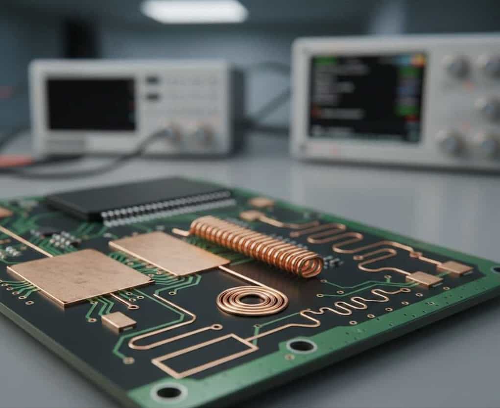
- Trace antennas offer low cost and high integration.
- Chip antennas save space but require precise matching circuits.
- Wire antennas provide better gain but increase assembly complexity.
But wait, there is a catch.
Key Takeaway
Selecting the right antenna type early prevents major layout overhauls and ensures your RF PCB Assembly meets its range targets.
| Antenna Type | Cost | Size | Performance |
| Trace | Very Low | Large | Moderate |
| Chip | Moderate | Very Small | High (if tuned) |
| Wire | Moderate | Variable | Very High |
Proper selection is the first step toward RF success.
What Role Does pcb antenna simulation Play in RF Reliability?
The pcb antenna simulation process allows engineers to predict how electromagnetic fields will interact with the board’s traces and surrounding components before a single board is manufactured. It acts as a virtual lab to refine radiation patterns and return loss.
Is Simulation Really Necessary for Every Design?
You will find that for high-frequency applications, even a 0.1mm shift in trace width can detune an antenna completely. Simulation helps you identify these sensitivities early, saving you from expensive Prototype PCB Assembly Service failures.
- Identifies resonant frequency shifts.
- Visualizes radiation patterns and gain.
- Predicts interference from nearby metal parts.
You might be wondering, how accurate can it be?
Key Takeaway
Detailed pcb antenna simulation reduces the number of prototyping cycles and guarantees faster time-to-market.
| Simulation Goal | User Benefit |
| VSWR Analysis | Optimizes power transfer |
| Gain Plots | Predicts communication range |
| Current Density | Identifies losses |
Simulating early prevents failing late.
How to Optimize Layout for pcb antenna simulation Performance?
Optimization involves creating a dedicated “keep-out” zone and ensuring a solid ground plane to act as a counterpoise for the antenna. The layout must be clean, avoiding any digital noise sources near the sensitive RF path.
Why Is Grounding the Secret to Antenna Efficiency?
You need a clear ground return path to ensure the antenna resonates at the intended frequency. For many trace antennas, the ground plane is actually half of the antenna system, and its size directly influences performance.
- Maintain a consistent “Keep-out” area around the radiator.
- Use multiple vias to tie ground planes together.
- Keep noisy digital traces far away from the RF section.
Think of it this way.
Key Takeaway
A disciplined layout approach, validated by pcb antenna simulation, ensures the antenna radiates efficiently without being smothered by board noise.
| Layout Feature | Purpose |
| Keep-out Zone | Prevents signal detuning |
| Ground Vias | Minimizes parasitic inductance |
| Signal Shielding | Reduces EMI interference |
Clean layouts lead to clear signals.
Why Is Impedance Control Essential in High-Frequency PCBA?
Impedance control ensures that the RF signal travels from the transceiver to the antenna without reflecting back and wasting energy. This is usually set to a standard 50 ohms to match most RF components.
How Do You Achieve Perfect 50-Ohm Matching?
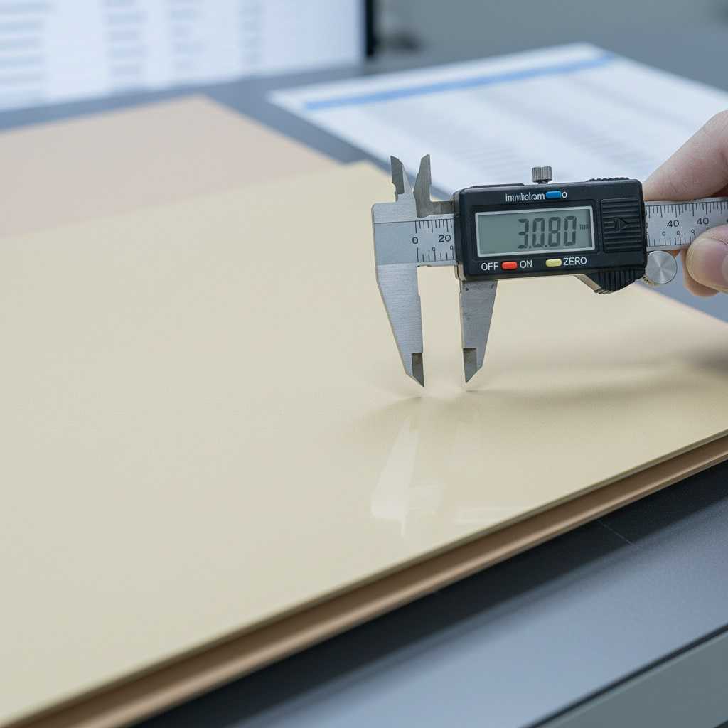
You must calculate trace widths based on the dielectric constant of the PCB material and the stack-up height. During High-Frequency PCB Assembly Service, manufacturers must maintain tight tolerances to keep this impedance stable.
- Use high-quality substrates like Rogers or High-Tg FR4.
- Implement Pi-matching networks for fine-tuning.
- Minimize the length of the RF feed line.
Does that make sense?
Key Takeaway
Precise impedance control, checked via pcb antenna simulation, maximizes power delivery and extends battery life by reducing signal reflections.
| Matching Element | Function |
| Series Inductor | Shifts resonance down |
| Shunt Capacitor | Adjusts impedance |
| Feed Line Width | Sets baseline impedance |
Matching is the bridge between the chip and the air.
What Impact Does Substrate Material Have on pcb antenna simulation?
The substrate’s dielectric constant ($D_k$) and loss tangent ($D_f$) determine how much signal is absorbed by the board itself. Lower loss materials are required as you move into the GHz range to maintain efficiency.
Should You Upgrade to High-Frequency Laminates?
You will find that for 5GHz or 24GHz designs, standard FR4 becomes too “leaky,” absorbing your precious RF energy as heat. Using specialized RF laminates ensures your pcb antenna simulation results actually match the physical performance.
- Rogers materials offer superior $D_k$ stability.
- Polyimide is useful for flexible antenna applications.
- Ceramic-filled laminates provide low loss at millimeter waves.
Here is the real kicker.
Key Takeaway
Choosing the correct substrate is the only way to ensure your Mixed Technology PCB Assembly remains efficient at high frequencies.
| Material | Loss Tangent (Df) | Ideal Frequency |
| Standard FR4 | 0.02 | < 1 GHz |
| High-Tg FR4 | 0.01 | 1 – 3 GHz |
| Rogers 4350B | 0.0037 | > 3 GHz |
Material science is the foundation of RF engineering.
How Does Enclosure Material Affect pcb antenna simulation Results?
Metal enclosures or metallic paints will block RF signals entirely, while plastics can shift the resonant frequency. Your antenna doesn’t live in a vacuum; it lives inside a product housing that interacts with its fields.
Can Your Choice of Plastic Detune Your Antenna?
You need to account for the enclosure’s permittivity in your pcb antenna simulation. Even a few millimeters of plastic clearance can change the effective length of the antenna, requiring a retuning of the matching network.
- Avoid metal coatings near the antenna area.
- Account for the “loading effect” of the housing.
- Test with the final industrial design in place.
It’s a delicate balance.
Key Takeaway
Simulating the antenna inside its final enclosure is the only way to avoid disappointing performance in the real world.
| Housing Material | RF Impact |
| ABS Plastic | Minor frequency shift |
| Aluminum | Total signal blockage |
| Carbon Fiber | High attenuation |
The “box” is part of the antenna system.
What are the Best Practices for RF Feed Line Routing?
The feed line is the highway for your RF signal, and any sharp turns or discontinuities act like roadblocks. Routing should be as direct as possible, using curved traces instead of 90-degree angles.
Why Avoid Vias in the RF Path?
You will find that every via adds parasitic inductance and capacitance, which can ruin your impedance matching. If you must use a via to reach another layer, ensure it is surrounded by a “ground stitched” cage to maintain shielding.
- Use microstrip or grounded coplanar waveguide (GCPW) designs.
- Maintain a constant distance to neighboring ground copper.
- Keep the feed line as short as humanly possible.
You’re probably thinking about the complexity.
Key Takeaway
Direct, shielded routing, verified by pcb antenna simulation, keeps your signal clean and prevents unwanted EMI emissions.
| Routing Type | Shielding | Ease of Design |
| Microstrip | Low | Easy |
| Stripline | High | Hard |
| GCPW | Excellent | Moderate |
Direct paths equal low losses.
How to Test and Validate pcb antenna simulation in Production?
Production testing ensures that every board leaving the factory meets the RF performance seen in the simulation. This usually involves measuring the Return Loss ($S_{11}$) using a Vector Network Analyzer (VNA).
Is 100% RF Testing Possible for Mass Production?
You should implement a “golden board” reference and use a test fixture with pogo pins to quickly check resonance. For high-volume SMT PCB Assembly, this automated check ensures that assembly variations haven’t detuned the product.
- Measure $S_{11}$ to check resonance and bandwidth.
- Use anechoic chambers for final radiation pattern validation.
- Implement functional OTA (Over-The-Air) tests.
But wait, there’s a better way.
Key Takeaway
Automated RF testing in pcb antenna simulation environments guarantees that every customer gets a device with a strong, stable connection.
| Test Equipment | Metric Measured |
| VNA | Impedance and $S_{11}$ |
| Spectrum Analyzer | Harmonic emissions |
| Power Meter | Transmit strength |
Verification is the final step in the RF journey.
What are the Common pcb antenna simulation Design Mistakes?
Most RF failures stem from “common sense” mistakes, like placing an antenna too close to a high-speed processor or a large capacitor. These errors create noise that drowns out weak wireless signals.
Are You Placing Components Too Close?
You need to respect the near-field zone of the antenna. Placing a metal shield or a switching power supply within this zone will distort the radiation pattern and reduce efficiency.
- Don’t route digital signals directly under the antenna.
- Avoid “floating” copper planes that aren’t grounded.
- Don’t use standard FR4 for millimeter-wave designs.
You see the pattern here.
Key Takeaway
Learning from common pcb antenna simulation pitfalls through DFM / DFA Engineering saves you from the “it works on the bench but not in the field” nightmare.
| Mistake | Consequence |
| No Ground Clearance | Zero radiation |
| Poor Impedance | Signal reflection |
| Digital Noise | Reduced sensitivity |
Experience is the best teacher in RF design.
How to Choose an Assembly Partner for RF Projects?
RF projects require an assembly partner that understands more than just soldering; they must understand the physics of high-frequency signals. Tight tolerances and specialized materials require a high level of process control.
Does Your Manufacturer Have RF Experience?
You will benefit from a partner that offers Turnkey PCB Assembly with dedicated RF testing stations. They should be able to provide X-ray inspection to ensure that internal vias in your antenna path are perfectly plated.
- Look for advanced AOI and X-ray capabilities.
- Check their experience with RF laminates like Rogers.
- Ensure they can perform functional RF validation.
This is the final piece of the puzzle.
Key Takeaway
A specialized pcb antenna simulation partner turns a complex RF design into a scalable, high-yield reality.
| Requirement | Why It Matters |
| Precision SMT | Critical for chip antennas |
| X-Ray Inspection | Checks buried RF vias |
| VNA Testing | Final quality assurance |
The right partner brings your RF vision to life.
Conclusion
Designing a successful PCB antenna is a balance of art and science, requiring precise pcb antenna simulation and a deep understanding of manufacturing tolerances. By following these guidelines—optimizing your layout, controlling impedance, and choosing the right substrate—you can overcome the challenges of high-frequency communication. We have addressed the critical pain points of signal loss and interference, providing a clear path to high-performance wireless products.
As an engineer-led factory, we specialize in bringing these complex designs to market with zero compromise on quality. Whether you need a simple BLE trace or a complex 5G array, our team is ready to support your production journey. Contact us today for a comprehensive review of your next RF project and ensure your connectivity is built to last. Our mission is to bridge the gap between world-class simulation and flawless hardware execution.
FAQ
Can I design a PCB antenna on standard FR4?
Yes, you can. However, FR4 is only recommended for frequencies below 1 GHz due to high signal loss. For 2.4 GHz WiFi or Bluetooth, you must use a high-quality, high-Tg FR4 and carefully tune the matching network. For anything higher, specialized RF laminates are essential.
What is the best way to tune a PCB antenna?
The best method is using a Vector Network Analyzer (VNA) to measure the $S_{11}$ (return loss). You then adjust the Pi-matching network (capacitors and inductors) until the resonant frequency matches your target and the impedance is as close to 50 ohms as possible.
How do I know if I need a chip antenna or a trace antenna?
If space is your biggest constraint, a chip antenna is the better choice. If cost is your primary concern and you have enough board real estate, a trace antenna (like an Inverted-F) is the way to go, as it costs nothing in components.
Does the thickness of the PCB affect the antenna?
Absolutely. The PCB thickness changes the dielectric distance between the trace and the ground plane, which directly impacts the characteristic impedance. You must account for the exact board thickness in your impedance calculations and simulation.
What types of aluminum casting are used for RF housings?
Different types of aluminum casting, such as die-casting, are often used for RF enclosures because they provide excellent EMI shielding. While the housing material doesn’t affect the PCB assembly directly, it must be considered in the overall antenna system design to prevent signal blocking.