
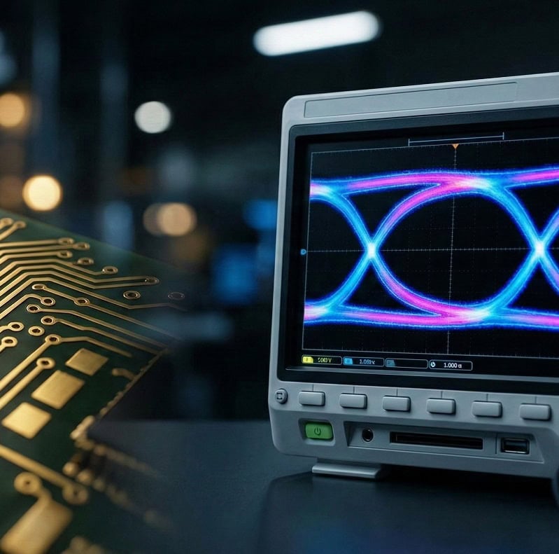
An eye diagram serves as a critical diagnostic tool in high-speed electronics by overlaying multiple traces of a digital signal to visualize its timing and amplitude health. Here’s the deal: without this visual confirmation, your high-speed design remains a gamble against physics.
Imagine spending months perfecting a complex multi-layer board only to find it fails intermittently in the field. You test the traces, but everything looks “fine” on a standard oscilloscope. The frustration mounts as deadlines loom and your client’s patience thins. This is where precision analysis saves the day. We provide a clear path forward by utilizing advanced signal integrity simulations and testing protocols to ensure every bit reaches its destination. Our engineering team at Queen EMS has successfully navigated these high-speed hurdles for global telecom and industrial leaders, proving that a proactive approach to signal quality is the only way to avoid costly re-spins.
1. What Is an Eye Diagram in High-Speed PCB Design?
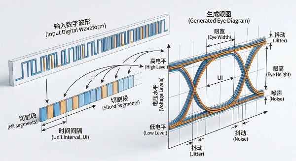
An eye diagram is a visual representation of high-speed digital signals where individual bit periods are sliced and layered on top of each other. This composite image allows engineers to see the statistical variation in signal performance at a single glance. You might be wondering why we don’t just look at a single pulse. A single pulse won’t reveal the hidden cumulative effects of jitter or noise that occur over millions of cycles.
How Does the Overlay Process Work?
The oscilloscope captures the data stream and triggers at every clock cycle, effectively folding the long string of bits into a single UI (Unit Interval). This process reveals how consistent the “1s” and “0s” are across time.
- It captures every signal transition point.
- It overlays voltage levels for high and low states.
- It reveals the timing precision of the sampling clock.
Why Is It Shaped Like a Human Eye?
The distinct shape forms because the transitions between high and low states naturally converge at the edges of the bit period and spread out in the middle. If the signal is clean, the middle of the display remains wide open, resembling an open eye. But here’s the kicker: if the eye starts to “close,” your data integrity is officially in danger.
| Parameter | Visual Feature | Physical Meaning |
| Eye Height | Vertical Opening | Noise Margin / Signal Amplitude |
| Eye Width | Horizontal Opening | Timing Margin / Jitter Tolerance |
| Eye Crossing | Intersection Point | Duty Cycle Distortion |
This table illustrates how visual cues directly translate to physical signal properties on your board.
Key Takeaway
Understanding the basic structure of the eye allows you to quickly identify if your high-speed channel is fundamentally sound or failing.
2. How Does Intersymbol Interference Affect the Eye Diagram?
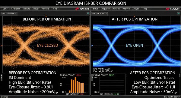
Intersymbol interference (ISI) occurs when previous signal pulses leak into the current bit period, distorting the waveform and narrowing the eye. An eye diagram clearly shows this as a blurring of the signal lines, making the “1” and “0” levels less distinct. What’s the real story? ISI is often the primary reason high-speed designs fail compliance even when the layout looks perfect.
What Causes Pulse Spreading?
The primary culprit is the limited bandwidth of the PCB traces, which acts like a low-pass filter on the square waves. This causes the edges of the pulses to round off and “smear” into the neighboring time slots.
- Skin effect increases trace resistance at GHz speeds.
- Dielectric loss absorbs electrical energy from the signal.
- Excessive trace length creates more opportunities for attenuation.
Can We Mitigate ISI Through Layout?
Managing ISI requires a combination of proper impedance control and the use of high-quality base materials that offer lower dissipation factors. By reducing the energy loss, we keep the pulse transitions sharp and the eye wide open. Ready for the good part? Using advanced mixed-assembly techniques ensures that the transition from chip to board doesn’t introduce extra parasitic capacitance.
| Signal Rate | Recommended Material | ISI Risk Level |
| < 3 Gbps | Standard FR-4 | Moderate |
| 5 – 10 Gbps | Mid-Loss Materials | High |
| > 10 Gbps | Low-Loss High-Speed | Critical |
Choosing the right material substrate is the first line of defense against pulse spreading and ISI-related failures.
Key Takeaway
Visualizing ISI through an eye pattern helps you decide if you need to upgrade your PCB material or implement equalization.
3. Why Is Bit Error Rate Linked to the Eye Diagram?
The bit error rate (BER) represents the probability of a receiver misinterpreting a “1” as a “0” or vice versa. An eye diagram provides a visual “safety zone” where the larger the opening, the lower the BER will likely be. This is where it gets interesting: a small eye opening doesn’t just look bad; it mathematically guarantees that your system will lose data.
How Does Noise Margin Play a Role?
The vertical height of the eye represents the noise margin, which is the amount of electrical noise the signal can withstand before a bit flip occurs. If the height is too small, even a tiny amount of crosstalk can trigger an error.
- Thermal noise is a constant presence in circuits.
- Power plane switching noise can induce voltage ripples.
- External EMI can inject noise into the signal path.
Is Timing Uncertainty a Factor?
Horizontal eye closure is a direct result of timing jitter, which shifts the transition points and reduces the time the receiver has to sample the bit. If the sampling clock hits the transition region instead of the stable center, the bit value becomes unpredictable. Let’s look closer: even a small reduction in eye width can lead to a massive increase in BER.
| Eye Opening % | Estimated BER | Performance Rating |
| 90% | < 10^-12 | Excellent |
| 70% | 10^-9 | Acceptable |
| 40% | 10^-3 | System Failure |
A wider eye opening provides a robust buffer against the unpredictable noise found in real-world operating environments.
Key Takeaway
Monitoring the eye opening allows you to predict and prevent data loss before the hardware reaches the end-user.
4. What Role Does Jitter Play in Eye Diagram Closure?
Jitter is the deviation of a signal’s transitions from their ideal positions in time. On an eye diagram, jitter manifests as thick, fuzzy vertical lines where the signal transitions from high to low. Here is the deal: if your clock source isn’t stable, your eye diagram will never look clean, regardless of your layout.
What Is Deterministic vs Random Jitter?
Deterministic jitter is predictable and usually caused by system phenomena like crosstalk or reflection. Random jitter, however, follows a Gaussian distribution and is often caused by thermal noise within the components.
- Crosstalk jitter originates from traces in close proximity.
- Duty cycle distortion alters the timing symmetry.
- Random jitter is a physical property of all conductors.
How Do We Control Jitter in PCB Layout?
To minimize jitter, you must ensure ultra-stable power delivery and use high-precision oscillators. Furthermore, maintaining consistent differential pair lengths is vital to prevent skew, which is a major contributor to jitter. Think about this: a difference of just a few mils in trace length can be the difference between a pass and a fail at high speeds.
| Jitter Type | Main Cause | Mitigation Strategy |
| Periodic Jitter | Switching Supplies | Better Decoupling |
| Data-Dependent Jitter | ISI / Reflections | Impedance Matching |
| Bounded Jitter | Crosstalk | Increase Trace Spacing |
Identifying the specific “flavor” of jitter on the eye allows for targeted troubleshooting during the prototype phase.
Key Takeaway
Minimizing jitter is essential for keeping the eye wide horizontally, ensuring the receiver has a stable window to read data.
5. Can Eye Mask Testing Ensure Channel Compliance?
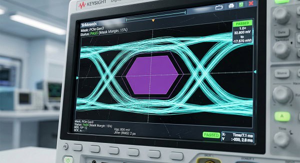
Eye mask testing involves placing a “forbidden” hexagonal or rectangular shape in the center of the eye diagram to define the limits of acceptable performance. If any part of the signal trace touches or enters this mask, the eye diagram indicates a compliance failure. It’s no secret that industry standards rely heavily on these masks for certification.
What Defines the Mask Shape?
The dimensions of the mask are dictated by the specific protocol standards, such as HDMI, Ethernet, or DDR. These shapes account for the minimum voltage and timing requirements the receiver needs to operate reliably.
- The center box sets the minimum voltage threshold.
- Top and bottom regions set the maximum voltage peaks.
- Mask sizes are updated as protocol speeds increase.
What Happens if the Signal Hits the Mask?
A mask hit means the signal integrity is compromised, and the device will likely experience data corruption or link drops. This usually triggers a design review to identify if the issue is in the silicon, the connector, or the PCB traces. But wait, there’s more: even if you pass the mask, a “tight” pass suggests your design lacks the headroom needed for mass production.
| Protocol | Typical Mask Height | Typical Mask Width |
| USB 3.x | 100 mV | 0.6 UI |
| PCIe Gen 4 | 15 mV | 0.3 UI |
| 10G Ethernet | 95 mV | 0.7 UI |
Strict adherence to mask testing ensures that your PCB will work seamlessly with other compliant devices in the ecosystem.
Key Takeaway
Mask testing provides a definitive “Pass/Fail” metric that simplifies the complex world of high-speed signal validation.
6. How Do Reflections Distort the Eye Diagram?
Reflections occur when a signal encounters an impedance mismatch, causing part of the energy to bounce back toward the source. On an eye diagram, reflections appear as “ringing” or “overshoot” on the top and bottom of the eye. Believe it or not, even a small via can act as a mirror for high-frequency signals.
Where Do Reflections Usually Start?
Mismatches typically happen at connectors, IC pins, or where a trace changes layers without a proper return path. These discontinuities create standing waves that distort the original signal shape and close the eye.
- Improperly terminated traces create large reflections.
- Stub vias create resonance points that trap energy.
- Sudden changes in trace width create impedance steps.
How Can We Clean Up These Artifacts?
The solution lies in rigorous impedance matching and the use of “back-drilling” to remove via stubs. Ensuring a continuous reference plane under the trace is also mandatory for maintaining the signal’s consistent environment. Here’s the kicker: we use advanced medical-pcb-assembly standards to ensure the highest reliability against reflections.
| Reflection Cause | Visual Effect | Fix |
| Un-terminated Line | Massive Overshoot | Add Termination |
| Via Stub | Narrowing of Eye | Back-drilling |
| Width Change | Waveform “Steps” | Constant Width |
Controlling reflections is the only way to keep the eye “clean” and prevent false triggers at the receiver end.
Key Takeaway
Eliminating reflections through precise layout keeps the eye’s edges sharp and prevents voltage violations.
7. What Is the Difference Between Real-Time and Equivalent-Time Sampling?
To generate an eye diagram, oscilloscopes use either real-time sampling for lower speeds or equivalent-time sampling for ultra-high frequencies. You might be wondering which one is better for your specific PCB project. The choice depends entirely on the data rate and whether you need to capture transient, one-time events.
When Is Real-Time Sampling Used?
Real-time oscilloscopes capture a single long record of data at an extremely high sample rate. This is great for seeing how the eye changes over time or capturing “glitches” that happen only once.
- It captures non-repetitive data streams accurately.
- It allows for analysis of transient glitches.
- It is ideal for debugging protocol-level handshake errors.
Why Is Equivalent-Time Sampling Preferred for Very High Speeds?
Equivalent-time (sampling) oscilloscopes build the eye by taking samples from many different repetitions of the signal. This allows for much higher effective bandwidth and lower noise, making it the gold standard for high-performance lanes. This is where it gets interesting: if your signal isn’t repetitive, a sampling scope will give you a completely garbled eye.
| Scope Type | Max Bandwidth | Best For |
| Real-Time | Up to 100 GHz | Troubleshooting |
| Sampling | 100+ GHz | Compliance |
Understanding your measurement tool is just as important as the PCB design itself when it comes to validating signal health.
Key Takeaway
Selecting the right sampling method ensures that the eye diagram you see accurately represents the physical reality of your board.
8. How Does Equalization Open a Closed Eye Diagram?
Equalization is a technique used to compensate for the frequency-dependent losses in a PCB channel, effectively “opening” an eye that would otherwise be closed. An eye diagram taken before equalization may look like a mess, while the post-equalized eye is perfectly clear. The good news is that most modern high-speed chips have these tools built right in.
What Are CTLE and DFE?
Continuous time linear equalization (CTLE) boosts high-frequency components at the receiver to counteract trace loss. Decision feedback equalization (DFE) uses a more complex algorithm to cancel out ISI based on previously received bits.
- CTLE is efficient and used for moderate losses.
- DFE can correct for complex reflections.
- Combined usage is standard for high-speed Ethernet.
Can We Equalize at the Transmitter?
Yes, this is known as “pre-emphasis” or “de-emphasis”. The transmitter artificially boosts the high-frequency transitions before they even enter the PCB trace, so they arrive at the receiver with a more balanced profile. What’s the real story? Without pre-emphasis, long backplanes would be nearly impossible to use for data.
| EQ Type | Location | Primary Benefit |
| Pre-emphasis | Transmitter | Offsets Loss |
| CTLE | Receiver | Vertical Opening |
| DFE | Receiver | Eliminates ISI |
Equalization is like an “active lens” that brings a blurry signal back into sharp focus for the receiver.
Key Takeaway
Using equalization allows engineers to push data through copper traces that would otherwise be physically incapable of supporting high speeds.
9. Why Does Differential Skew Ruin the Eye Diagram?
Differential signals rely on two traces carrying equal and opposite signals; skew happens when one of these signals arrives later than the other. On an eye diagram, skew causes the crossing points to become asymmetric and reduces the overall eye height. But here’s the kicker: even a tiny “snake” in your trace layout can introduce enough skew to kill a high-speed link.
How Does Skew Convert to Common-Mode Noise?
When the two halves of a differential pair are out of sync, they no longer cancel each other’s electromagnetic fields. This creates common-mode noise, which can cause the board to fail EMI testing and increase jitter.
- Inconsistent dielectric constants create velocity mismatches.
- Trace bends create unavoidable path length differences.
- Dense routing forces asymmetrical pair geometries.
How Do We Fix Skew in Practice?
Engineers use “phase matching” to add small amounts of length to the shorter trace. We also recommend using “spread glass” PCB materials to ensure the signal sees a consistent dielectric constant. Ready for the good part? Our robotics clients have found that automated length-matching tools are essential for their complex signals.
| Skew Amount | Impact on Signal | Fix |
| < 1 ps | Negligible | None Required |
| 5 – 10 ps | Increased Jitter | Length Match |
| > 20 ps | Eye Closure | Redesign |
Precise phase alignment is the secret to maintaining the high signal-to-noise ratio required for modern data standards.
Key Takeaway
Eliminating skew ensures that your differential pairs work as a team, maximizing the vertical and horizontal eye opening.
10. How Can Simulation Predict the Eye Diagram Before Production?

Signal integrity (SI) simulation allows you to generate a virtual eye diagram before you ever commit to a physical prototype. You might be wondering if these simulations are actually accurate. When done correctly with high-quality models, simulations can predict hardware performance with incredible precision.
Why Simulate Instead of Prototype?
Prototyping high-speed boards is expensive and time-consuming. Simulation allows you to test “what-if” scenarios, such as changing trace widths or trying different dielectric materials, in a matter of minutes.
- It eliminates the need for trial-and-error prototyping.
- It identifies thermal or signal conflicts early.
- It verifies chip-to-chip compatibility.
What Is a Statistical Eye?
For extremely long data patterns, a standard transient simulation would take too long. Statistical simulation uses mathematical models to predict the eye shape over billions of bits in just seconds. This is where it gets interesting: it allows you to see the “tails” of the jitter distribution that only appear rarely.
| Simulation Type | Speed | Accuracy |
| SPICE | Slow | High (Circuit) |
| IBIS-AMI | Fast | High (System) |
| Channel | Very Fast | High (Statistical) |
Virtual prototyping through SI simulation is the most cost-effective way to guarantee “first-pass” success for high-speed designs.
Key Takeaway
Simulation takes the guesswork out of high-speed design, providing a clear roadmap to a wide-open eye and a reliable product.
Conclusion
Mastering the eye diagram is no longer optional for B2B engineers; it is the definitive gateway to ensuring signal integrity in an increasingly high-speed world. We have explored how this tool uncovers the hidden dangers of jitter, intersymbol interference, and reflections, providing a visual benchmark for channel compliance. By integrating simulation and advanced PCB materials, you can transform a failing, closed-eye design into a robust, high-performance system. At Queen EMS, we are committed to helping you bridge the gap between complex theory and reliable hardware. If you are ready to ensure your next project meets the highest standards of data integrity, contact us today to discuss your high-speed layout requirements. Let’s build something that stays “wide open” together.
Frequently Asked Questions
Q1: Can I see an eye diagram on a cheap oscilloscope? No, you typically cannot. High-speed eye diagrams require oscilloscopes with a bandwidth at least 3 to 5 times the fundamental frequency of your signal to capture the necessary harmonics.
Q2: What’s the best way to open a closed eye? Start with the basics. Check your impedance matching and trace lengths first, and if the eye remains closed due to unavoidable trace loss, enable the transmitter’s pre-emphasis or the receiver’s equalization settings.
Q3: How do I know if my eye diagram is “good enough”? Check the mask. If your signal never touches the industry-standard mask for your protocol (like PCIe or USB) and you have sufficient headroom in both height and width, your design is robust.
Q4: Can I use an eye diagram for low-speed signals? Yes, you can, but it is rarely necessary. For signals like I2C or low-speed UART, simple rise-time and voltage level checks are usually sufficient since ISI and jitter are negligible at those frequencies.
Q5: How do I know if jitter is the main problem? Look at the vertical crossing points. Thick, fuzzy vertical lines at the crossing points indicate high jitter, while blurred horizontal levels at the top and bottom suggest noise or ISI issues.