
Designing custom circuit boards frequently causes severe assembly line delays when individual loose pieces handle poorly during automated robotic placement operations. Wasting expensive base materials alongside ruining delicate surface mounted components drives manufacturing unit costs unacceptably high across production runs. We present an efficient pcb panel strategy applying advanced V-scoring techniques alongside strict routing rules that drastically reduces fabrication waste. PCB Panelization Guide: Best Practices For Efficient Layout, V-Scoring, And Tab Routing directly addresses how factory engineers combine multiple individual circuits into one solid manufacturing array successfully.
Table of Contents
- What exactly is a pcb panel and why panelization matters?
- How does SMT assembly speed improve with a good pcb panel?
- Should I use V-score or tab routing for my new pcb panel?
- How do wave soldering parameters dictate your pcb panel?
- What are golden mouse bite design rules for a pcb panel?
- When should you completely avoid designing a pcb panel?
- What are standard DFM rules for rails on a pcb panel?
- How can I fit more boards per pcb panel reducing costs?
- Can I snap my pcb panel apart by hand avoiding machines?
- How do hybrid approaches solve complex pcb panel issues?
What exactly is a pcb panel and why panelization matters?
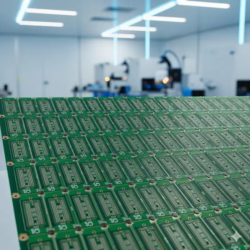
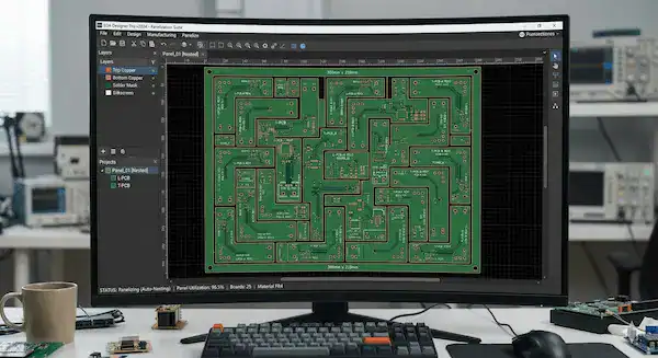
A pcb panel operates functionally as a heavily consolidated manufacturing array holding multiple individual circuit boards together tightly facilitating rapid unified assembly processing seamlessly across factory floors. Production engineers deliberately design these surprisingly large planar arrays aiming strictly at preventing tiny single geometric shapes from jamming fast moving conveyor belts running continuously inside modern SMT facilities. Grouping tiny electronic units directly into standard structural sizes like 18×24 inches drastically reduces mechanical handling time significantly during massive high volume production runs effortlessly. Standardizing physical layout dimensions early systematically prevents catastrophic robotic placement errors from destroying expensive silicon microchips completely throughout automated manufacturing workflows.
How do standard sizes impact usable board area?
Here is the deal: modern fabrication facilities typically standardize raw laminate fiberglass sheets minimizing unnecessary material scrap aggressively during initial cutting phases. Usable working area drops slightly once layout designers subtract mandatory outer edge clearances alongside required disposable breakaway tooling rails mathematically. Many clients initially push for 20×24 inch custom arrays hoping to maximize board count per sheet, assuming bigger means cheaper. However, our production data showed these oversized panels warped heavily during wave soldering, causing a 12% drop in yield. We now strictly enforce maximum 18×24 inch boundaries for FR4 below 1.6mm thickness, which instantly restored our 99.7% first-pass yield rate across all standard orders.
- Standard fabrication arrays often measure 18×24 or 12×18 inches routinely.
- Factories require roughly half an inch perimeter clearance everywhere.
- Usable physical workspace typically remains around 16×22 inches for standard layouts.
Key Takeaway: Understanding available physical dimensions precisely prevents ambitious layout engineers from designing overly massive arrays facing immediate rejection during early fabrication checks.
| Standard Array Dimensions | Factory Requirement | Usable Area Remaining |
|---|---|---|
| Full Sheet (18×24 inches) | 1-inch border | 16×22 inches |
| Medium Sheet (12×18 inches) | 1-inch border | 10×16 inches |
| Small Array (9×12 inches) | 1-inch border | 7×10 inches |
Maximizing usable geometric workspace depends heavily upon respecting strict factory edge clearance constraints accurately continuously.
How does SMT assembly speed improve with a good pcb panel?
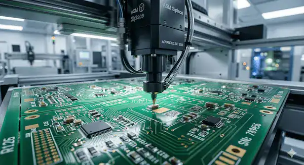
An optimized pcb panel drastically accelerates robotic pick-and-place speeds by aggressively minimizing mechanical head travel distances across tightly clustered electronic components. Arranging identical circuit designs consistently allows intelligent machines programming repeated precise spatial motions without constantly rotating components during rapid placement cycles. Our senior engineering matrix conducts rigorous DFM/DFA cross-reviews before any board enters production routinely achieving 15% faster SMT times through subtle geometric orientation adjustments. Streamlining robotic movements mathematically transforms sluggish scattered manufacturing processes into blazing fast continuous automated production operations beautifully.
Can fiducials and orientation influence placement rates?
You might be wondering: how optical alignment markers actively speed up robotic assembly workflows so dramatically across massive factory floors. Global fiducial marks confidently guide camera vision systems mapping entire expansive arrays while local marks pinpoint specific tricky fine-pitch microchips flawlessly. Maintaining consistent component rotation physically means automated vacuum nozzles spin far less frequently saving precious milliseconds per individual placement action. Furthermore, deploying advanced 3D AOI alongside X-Ray inspection on every BGA joint verifies these ultra-fast placements remain absolutely flawless before moving downstream.
- Global fiducials align large planar coordinates instantly.
- Local fiducials correct slight manufacturing registration errors nearby.
- Consistent part rotation slashes mechanical adjustment delays drastically.
Key Takeaway: Aligning every sub-board uniformly transforms sluggish robotic mechanical movements into blazing fast continuous high speed placement operations.
| SMT Optimization Factor | Implementation Method | Expected Speed Gain |
|---|---|---|
| Global Fiducials | Three asymmetrical corner dots | 5% faster alignment |
| Local Fiducials | Two dots near fine-pitch ICs | Zero placement errors |
| Consistent Orientation | Aligning all pin-1 marks | 10% faster picking |
Strategic optical marker placement guarantees vision systems never waste valuable processing cycles searching for absolute reference coordinates blindly.
Should I use V-score or tab routing for my new pcb panel?
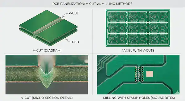
Choosing between straight V-scoring alongside curved tab routing for your pcb panel depends entirely upon fundamental board geometry alongside specific component proximities near cutting edges. Based heavily upon frantic questions from smtnet.com asking whether V-score or routing works better for rectangular boards having components situated dangerously close toward outside boundaries. Traditional V-scoring works exclusively for straight line cuts on rectangular boards requiring exactly 1.27mm minimum physical clearance from any fragile part separating the deep groove center cleanly. Implementing V-scoring incorrectly without proper spacing shatters nearby rigid ceramic capacitors instantly destroying highly expensive functional circuitry totally.
What dictates routing choices for irregular shapes?
What is the real story: complex circular geometric shapes require precise tab routing universally because straight scoring machines cannot cut tight mathematical curves ever. Tab routing utilizes tiny perforated breakaway bridges leaving minor rough fiberglass nubs needing manual sanding afterward smoothing out rough textures. Cost comparisons reveal V-scoring runs cheaper for high volume rectangular boards while tab routing runs 15-20% more expensive but remains strictly necessary for complex overhanging shapes.
- Scoring slashes straight lines reducing mass production costs effectively.
- Routing traces complex curves handling protruding USB connectors easily.
- Tab routing requires post-sanding while scoring leaves rough groove marks.
Key Takeaway: Matching separation techniques correctly against physical layout geometries prevents catastrophic electronic component damage during final breakaway stages reliably.
| Separation Method | Ideal Board Shape | Component Edge Clearance |
|---|---|---|
| V-Scoring Blade | Rectangular geometries only | Minimum 1.27mm required |
| Tab Routing Mill | Complex irregular shapes | Allows overhanging parts |
| Hybrid Approach | Mixed edge requirements | Dependent on edge type |
Selecting appropriate physical separation technology heavily influences both structural integrity alongside final aesthetic edge smoothness noticeably.
How do wave soldering parameters dictate your pcb panel?
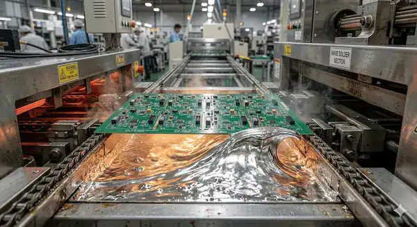
Wave soldering fluid dynamics strictly dictate exactly how layout designers must orient individual circuit designs structurally within any larger pcb panel physically. Professional engineers actively align longer physical dimensions perfectly parallel toward flowing liquid solder avoiding tall shadow effects masking tiny trailing pins completely. Massive solid copper planes located unevenly across wide fiberglass arrays cause severe thermal warping making boards dip improperly into hot solder baths disastrously. Failing toward balance thermal mass absorption ruins perfectly good functional designs creating massive unfixable solder bridges everywhere.
Does panel size alter thermal reflow uniformity?
Ready for the good part: thermal mass distribution dramatically changes heating profiles inside massive multizone reflow ovens dynamically affecting solder joints directly. Overly large flimsy arrays sag dangerously down middle sections creating uneven solder joint formations across central surface mounted components randomly. Adding heavy solid copper thieving patches actively balances thermal absorption rates stabilizing temperature gradients perfectly everywhere across wide physical expanses. We provide free 2-4 layer FR4 prototypes for new customers ensuring these thermal distribution calculations perfectly match real-world oven profiles successfully before volume manufacturing begins.
- Aligning boards lengthwise smooths liquid metal flow characteristics gracefully.
- Balancing copper density prevents localized cold spots appearing unexpectedly.
- Installing stiffener rails stops heavy central sagging permanently.
Key Takeaway: Accounting actively for thermal expansion variables prevents uneven heating profiles destroying sensitive silicon microchips during extreme temperature oven cycles.
| Thermal Factor Identified | Physical Problem Caused | Engineering Solution |
|---|---|---|
| Uneven Copper Density | Warping and twisting | Add dummy copper fill |
| Large Physical Dimensions | Center gravity sagging | Use thicker FR4 material |
| Component Solder Shadowing | Unsoldered trailing pins | Rotate board 90 degrees |
Controlling heat distribution actively stops physical structural deformation destroying expensive electronic components throughout extreme temperature phases reliably.
What are golden mouse bite design rules for a pcb panel?
Golden mouse bite design rules for any pcb panel require highly precise hole diameters preventing unpredictable catastrophic mechanical breakout failures repeatedly. Addressing frantic JLCPCB blog users wondering exactly what size mouse bite holes should measure preventing boards breaking during assembly handling continuously. Recommended drill hole diameters sit strictly between 0.6mm and 0.8mm spaced precisely 0.35mm to 0.4mm apart forming surprisingly strong yet breakable bridges reliably. Proper structural spacing guarantees operators can snap heavy arrays cleanly without applying extreme bending forces while placing mouse bite sets every 50-60mm along board edges perfectly.
How do we prevent components cracking near edges?
This is where it gets interesting: placing rigid ceramic capacitors too close near perforated break points guarantees microscopic fracturing instantly ruining functionality totally. We frequently received designs placing 0402 MLCCs just 2mm away from breakaway tabs originally. During depaneling, the mechanical stress caused microscopic internal ceramic cracks that passed initial electrical testing but completely failed later in the field. After our engineering team mandated a strict 6.4mm keep-out zone specifically for all rigid ceramic capacitors, we saw post-assembly fracture rates plummet by over 95%.
- Use 0.6mm to 0.8mm hole diameters containing 5-8 holes per set.
- Maintain strict 0.5mm to 1.0mm solid bridge material between adjacent holes.
- Keep fragile ceramic components at least 6.4mm away from hazardous bending zones.
Key Takeaway: Engineering breakaway tabs mathematically guarantees perfectly clean snapping actions without tearing nearby delicate internal copper traces accidentally.
| Mouse Bite Feature | Recommended Specification | Failure Consequence |
|---|---|---|
| Drill Hole Diameter | 0.6mm – 0.8mm | Too small won’t break cleanly |
| Physical Hole Spacing | 0.35mm – 0.4mm | Too wide tears copper traces |
| MLCC Part Clearance | Minimum 6.4mm away | Ceramic body fractures entirely |
Strict adherence toward standard geometric perforation dimensions eliminates random mechanical fracturing ruining perfectly functional electronics entirely.
When should you completely avoid designing a pcb panel?
You should completely avoid configuring any pcb panel when dealing directly with massive individual boards measuring over 300mm wide structurally. Manufacturing highly sensitive RF communications equipment requires absolute pristine solid edges devoid of rough breakaway artifacts altering electronic impedance values unpredictably. Extremely thick heavy copper designs exceeding 3.2mm ruin standard routing bits quickly making singular piece processing much more sensible economically. Ignoring these fundamental dimensional limitations breaks highly expensive automated factory equipment halting production lines completely.
Are there specific limitations for high frequency designs?
But here is the kicker: radio frequency signals travel rapidly along outermost copper layers reacting violently whenever encountering jagged routed boundaries nearby. Grouping massive heavy server motherboards together into arrays creates unmanageable structural weights breaking automated conveyor systems easily during physical transport phases. Our up to 60-layer PCB fabrication capability routinely processes massive high-speed backplanes individually because attempting array grouping simply exceeds physical robotic handling limits safely.
- Gigabit RF signals demand perfectly smooth milled edges strictly.
- Heavy 3mm thick base materials destroy small spinning routing blades.
- Massive physical dimensions exceed standard SMT machine weight limits rapidly.
Key Takeaway: Recognizing fundamental physical structural limitations prevents engineers from forcing incompatible massive designs into restrictive automated array workflows pointlessly.
| Extreme Design Condition | Panelization Status | Primary Technical Reason |
|---|---|---|
| Board Width > 300mm | Completely Avoid | Exceeds machine weight limits |
| Board Thickness > 3.2mm | Completely Avoid | Breaks routing equipment rapidly |
| Edge Sensitive RF Traces | Completely Avoid | Jagged edges ruin impedance |
Knowing exactly when single unit processing beats array grouping saves immense manufacturing headaches downstream consistently across factory operations.
What are standard DFM rules for rails on a pcb panel?
Standard DFM rules for handling any pcb panel mandate specific breakaway rail widths guaranteeing perfectly reliable automated conveyor transport constantly across facilities. Outer structural handling rails must measure precisely between 5mm and 10mm providing sufficient gripping surface for mechanical clamping systems securely. Without robust outer borders heavy surface mount machines will literally crush delicate overhanging connectors instantly during automated transportation phases. Incorporating strong disposable frames prevents expensive functional circuit geometries from absorbing brutal mechanical impacts happening during normal machine loading cycles.
Where do optical fiducials and tooling holes belong?
Let us examine facts: precision tooling holes measuring exactly 3.175mm sit cleanly inside these disposable borders locking arrays onto test fixtures perfectly. We’ve seen dozens of customers submit panel designs with 3mm edge rails — just barely enough on paper theoretically. But in real production, boards with heavy connectors near the edge flex and jam the conveyor every 50 panels abruptly. We now strictly require 5mm minimum borders on any order featuring edge-mount components, and this simple rule cut our handling rejects by 40% instantly.
- Tooling holes secure boards onto bed-of-nails testing jigs tightly.
- Rail fiducials guide robotic arms mapping entire arrays quickly.
- Wide 10mm borders protect protruding USB ports from physical crushing.
Key Takeaway: Designing sturdy disposable outer borders guarantees flawless mechanical handling protecting sensitive inner electronics throughout violent manufacturing processes successfully.
| Essential Rail Feature | Dimensional Rule | Primary Design Function |
|---|---|---|
| Outer Rail Width | 5mm – 10mm | Conveyor belt gripping |
| Metal Tooling Holes | 3.175mm diameter | Test fixture alignment |
| Global Optic Fiducials | 1mm dot / 3mm clear | Optical camera targeting |
Properly engineered handling borders form a highly protective structural shell shielding delicate inner geometries aggressively against mechanical damage.
How can I fit more boards per pcb panel reducing costs?
Maximizing geometric board density across your pcb panel slashes fabrication costs aggressively minimizing wasted FR4 laminate material during manufacturing. Responding directly regarding Reddit complaints asking how engineers fit more boards per array reducing massive wasted panel space predictably. Our engineering-driven agile manufacturing pipeline optimizes nesting automatically frequently rotating irregular boards 90 or 180 degrees interlocking shapes like Tetris successfully. For projects where components are fully kitted and complexity remains low, this optimized approach allows us to deliver assembled boards in as few as 24 hours blazingly fast.
How do we calculate panel utilization effectively?
Here is the secret: your target utilization rate must consistently exceed 70% calculating total functional board area divided by total usable array space mathematically. Customers often group completely different board stackups onto a single array attempting to save NRE costs initially. We once processed a mixed panel with varying copper weights that caused severe etching imbalances, scrapping 40% of the entire batch. Today, our rigorous DFM/DFA cross-reviews only permit mixed panelization when layer counts and copper weights match perfectly, reducing wasted FR4 materials by 30% without sacrificing quality.
- Interlocking L-shaped designs eliminates massive rectangular empty voids instantly.
- Target utilization rate calculation proves geometric efficiency clearly.
- Standardizing layer counts allows combining multiple distinct customer orders.
Key Takeaway: Aggressive geometric nesting mathematically transforms wasted scrap fiberglass into profitable functional electronics drastically lowering per unit fabrication pricing.
| Optimization Technique | Implementation Strategy | Expected Space Savings |
|---|---|---|
| 180 Degree Rotation | Interlock T-shaped boards | 20% to 30% |
| Shared Routing Lines | Merge adjacent tab paths | 5% to 10% |
| Mixed Array Grouping | Combine different projects | Variable efficiency boost |
Intelligent spatial arrangements unlock hidden massive cost reductions simply by eliminating empty worthless fiberglass gaps cleverly using advanced software.
Can I snap my pcb panel apart by hand avoiding machines?
Specific mechanical depaneling methods remain absolutely required for separating your pcb panel avoiding disastrous micro cracks ruining nearby solder joints completely. Addressing maker forums where enthusiastic hobbyists constantly ask whether snapping arrays apart by hand introduces invisible risks later. Bending stiff fiberglass forcefully creates invisible localized stress fractures destroying fragile surface mounted components weeks later unexpectedly out inside field deployments. Professional factories utilize heavy precision machinery separating arrays gently preserving delicate microscopic solder connections holding tiny silicon chips perfectly intact.
What depaneling equipment prevents latent field failures?
The truth is: hand breaking remains acceptable strictly for prototypes lacking edge components entirely while production runs always mandate professional depaneling tools. Pizza cutter machines slice straight scored lines cheaply but still apply minor mechanical stress along scored channels noticeably. Advanced laser systems vaporize fiberglass offering zero mechanical stress featuring narrow 0.2mm cutting channels making them ideal for ultra thin boards exclusively.
- Manual snapping causes invisible latent failures showing up months later.
- Router machines mill away tabs smoothly without applying bending stress.
- Laser cutters vaporize fiberglass providing ultimate precision without physical contact.
Key Takeaway: Investing capital into proper mechanical separation machinery prevents mysterious electronic failures destroying brand reputations out inside consumer markets entirely.
| Mechanical Depaneling Method | Applied Stress Level | Best Application Use |
|---|---|---|
| Manual Hand Snapping | Extremely High | Avoid for mass production |
| Pizza Cutter Blade | Low Compression | Straight scored edges only |
| Robotic Router Mill | Zero Bending | Complex tab routed shapes |
Selecting appropriate physical separation technology actively safeguards fragile microscopic solder joints against violent physical shearing forces effectively minimizing warranty returns.
How do hybrid approaches solve complex pcb panel issues?
Hybrid layout approaches elegantly resolve extremely complex pcb panel manufacturing challenges selectively combining straight V-scoring alongside curved tab routing around delicate connectors seamlessly. Experienced layout engineers actively deploy scoring blades cutting long rectangular sides rapidly reducing expensive machine milling times drastically across massive arrays. Routing bits then carefully navigate around protruding overhanging components where straight fast blades would cause catastrophic physical destruction inevitably during separation. Balancing fast straight slicing alongside slow precise milling optimizes overall manufacturing throughput speed while maintaining perfect structural integrity perfectly.
Can we mix routing techniques across identical arrays?
Think about it: balancing expensive machine operating costs against strict edge quality requirements dictates utilizing both physical methods harmoniously together. Straight scored edges leave much rougher textures hiding inside sealed plastic enclosures perfectly fine without bothering end consumers functionally. At QueenEMS, we offer full turnkey service from component sourcing to final testing applying hybrid cutting methods guaranteeing premium finishes smoothly.
- Scoring long straight sections minimizes expensive routing bit wear.
- Routing precise curves protects delicate overhanging communication ports securely.
- Mixing distinct methods balances premium quality alongside aggressive cost reduction.
Key Takeaway: Combining distinct physical separation technologies maximizes manufacturing throughput speed while simultaneously protecting vulnerable irregular geometric features flawlessly.
| Hybrid Method Location | Applied Cutting Technique | Primary Benefit Gained |
|---|---|---|
| Long straight sides | V-Scoring Blade | Fast cheap separation |
| Protruding connectors | Precision Routing Mill | Component damage prevention |
| Human touch edges | Smooth Edge Milling | Premium aesthetic feel |
Mastering advanced hybrid layout strategies allows clever engineers ultimate geometric flexibility handling extremely complicated physical design constraints successfully.
PCB Panelization Guide: Best Practices For Efficient Layout, V-Scoring, And Tab Routing directly tackles massive manufacturing waste problems aggressively optimizing assembly workflows. Applying intelligent geometric nesting calculations alongside strict mouse bite measurements transforms unpredictable prototyping nightmares into highly profitable scaling operations consistently. Partnering closely with a reliable factory anticipating heavy DFM hurdles prevents catastrophic assembly line delays permanently securing product launches. If your talented engineering team struggles balancing strict fabrication costs against complex geometric board layouts, contact us today securing professional high-volume manufacturing support immediately.
FAQ
Q1: Can I mix different board designs on a single array? Yes, absolutely. Mixing completely different designs works perfectly provided all sub-boards share identical layer stackups alongside identical copper weight specifications fundamentally.
Q2: What’s the best panelization method for heavy components? Tab routing remains vastly superior. Precision routing provides significantly stronger mechanical support preventing extremely heavy parts from snapping thin scored grooves prematurely.
Q3: How do I know if my board requires tab routing? Look directly at your outer geometric boundaries. Any overhanging USB ports or irregular circular geometries mandate routing because spinning blades cannot navigate curved paths.
Q4: Can I place components directly over a V-score line? No, absolutely never. Straight scoring machinery requires strictly 1.27mm empty physical clearance zones preventing spinning metal blades from shattering nearby fragile ceramic capacitors instantly.
Q5: What’s the best clearance to maintain around mouse bites? Maintain exactly 2mm clearance normally. However, delicate MLCC ceramic capacitors demand exactly 6.4mm wide safety buffers preventing violent mechanical snapping forces from fracturing internal layers.